Skill Enhancement Programme: Understanding Renewable Energy and Smart Transportation
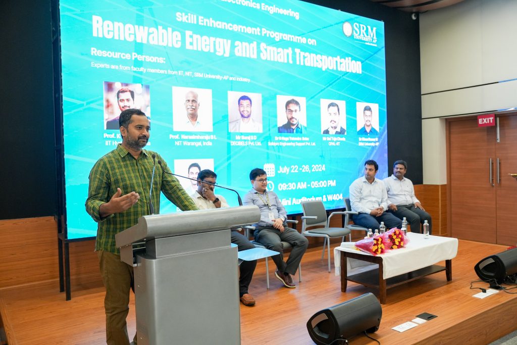
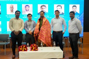
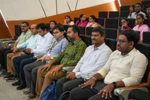
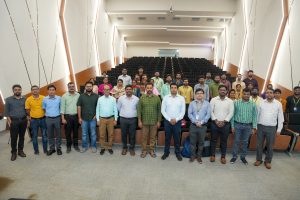
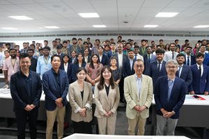
The Department of Electrical and Electronics Engineering hosted a highly successful five-day Skill Enhancement Programme on “Renewable Energy and Smart Transportation” from July 22 to July 26, 2024, signalling a major leap forward in addressing the vital sectors of electric vehicles and renewable energy systems. The programme conducted in a hybrid mode, featured live lectures, hands-on training, and interactive sessions, drawing a total of 50 participants. Chief Guest Dr K Sivakumar, HOD-EEE, IIT Hyderabad, highlighted the pressing need for such skill development initiatives and stressed the importance of keeping abreast of advancements in renewable energy and smart transportation.
Expert sessions on the emerging domains of Renewable Energy, including Advanced Power Conversion and Efficient Drives, Design and Simulation Tools, Battery Management and Charging Infrastructure, and Sustainability and Renewable Integration, fostered an in-depth understanding and application of the latest technologies in these fields.
Dr K Sivakumar started off the programme with an engaging session on advanced power conversion techniques and control strategies for electric vehicles. His insights into modern electric vehicle design set a strong foundation for the week. Participants gained a deep understanding and a solid theoretical base on the latest advancements in power converters and control techniques, which are crucial for the design and development of efficient electric vehicles.
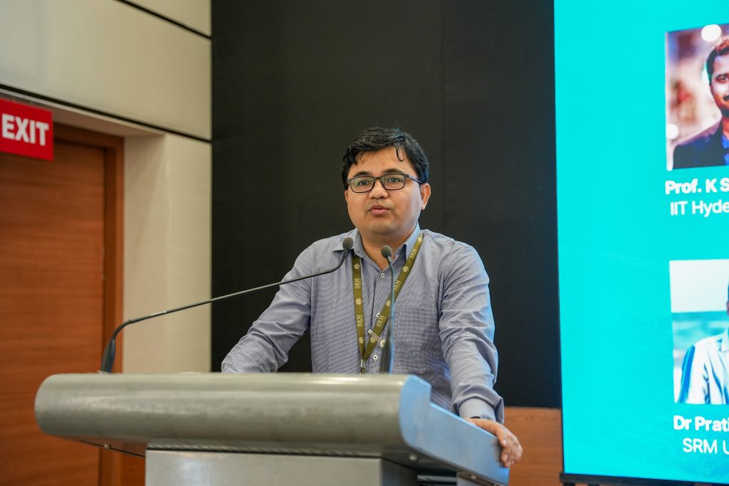
Subsequent technical sessions were led by esteemed experts from academia and industry, such as Dr Narasimharaju B L from NIT Warangal, Mr Suraj from Decibels Pvt. Ltd., Dr G Naga Yatendra Babu from Solidpro Engineering Support Pvt. Ltd., Mr Sai Teja Cherla from OPAL-RT, and Dr Kiran Kumar N, Dr Pratikanta Mishra from and Dr V Naresh Kumar from SRM University-AP.
Overall, the Skill Enhancement Programme provided participants with a comprehensive understanding of renewable energy and smart transportation, blending theoretical knowledge with practical skills and fostering discussions on current challenges and future opportunities in these fields.
- Published in Departmental Events, Departmental News, EEE, EEE NEWS, News
“From Andhra to Paris” – SRM AP’s Rising Star Selected for Paris Olympics 2024
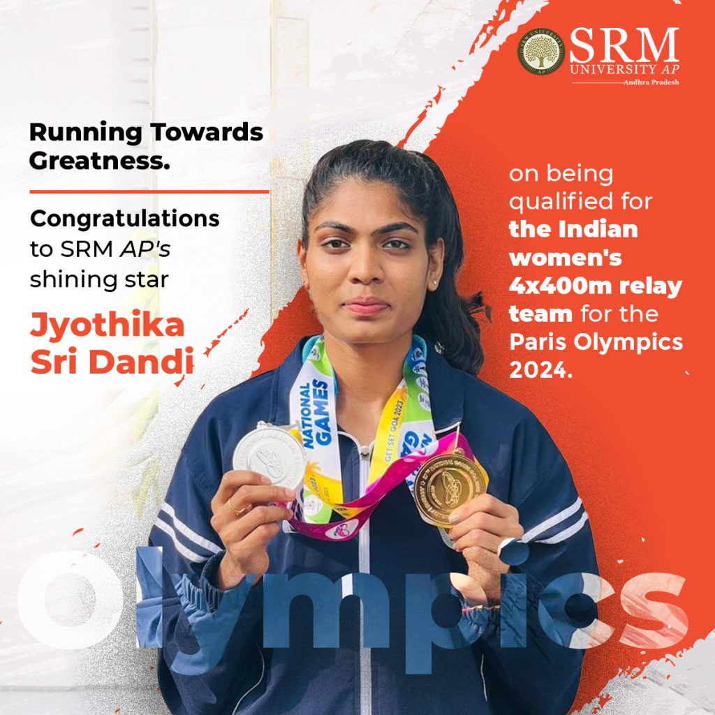
Ms Jyothika Sri Dandi, our first-year B.A. student at the Easwari School of Liberal Arts, has qualified for the Indian Women’s 4x400m Relay Team for the world’s foremost sports competition, the Paris Olympics 2024. Dr Dhiraj Parasher, Director–Sports, congratulated Ms Jyothika on this phenomenal achievement. He remarked, “To become an Olympian is a monumental mark in the career of an athlete. We are swelled with pride and offer unwavering support as we soundly believe that Jyothika will create history and return as an Olympic champion.”
Vice Chancellor Prof. Manoj K Arora also expressed his pride and zeal by stating, “Ms Jyothika is a national treasure that instils a belief and ambition in every young girl who dreams of being an Olympian. We, at SRM University-AP, wish her success and victory as she crafts her name in the tapestry of champions.”
Hailing from Tanuku town in the West Godavari district of Andhra Pradesh, the two-time national champion has paved her way to the elite sports championship through hard work, determination, and resilience.
Ms Jyothika had her breakthrough in 2021 when she secured Gold in the 400-metre race at the Indian U23 Championships. Her winning streak continued as she forged ahead to make her mark in 2023 by winning the Indian National Open Championships for 400 metres race in Thiruvananthapuram and winning bronze in the women’s 4 x 400 metres relay at the 2023 Asian Athletics Championships in Bangkok. Her blistering pace and performance at the 2024 World Relays Championships in Nassau, Bahamas, secured the Indian women’s relay team’s ticket to the Paris Olympics.
As the 2024 Paris Olympics unfolds, it is a moment of pride and anticipation for SRM University-AP as the institute extends its heartfelt wishes to Ms Jyothika and the Indian contingent representing our nation on this monumental platform.
- Published in News, Sports News, student affairs news, Students Achievements
“Nano Jatha”: A Pathway to Nanoscience and Technology
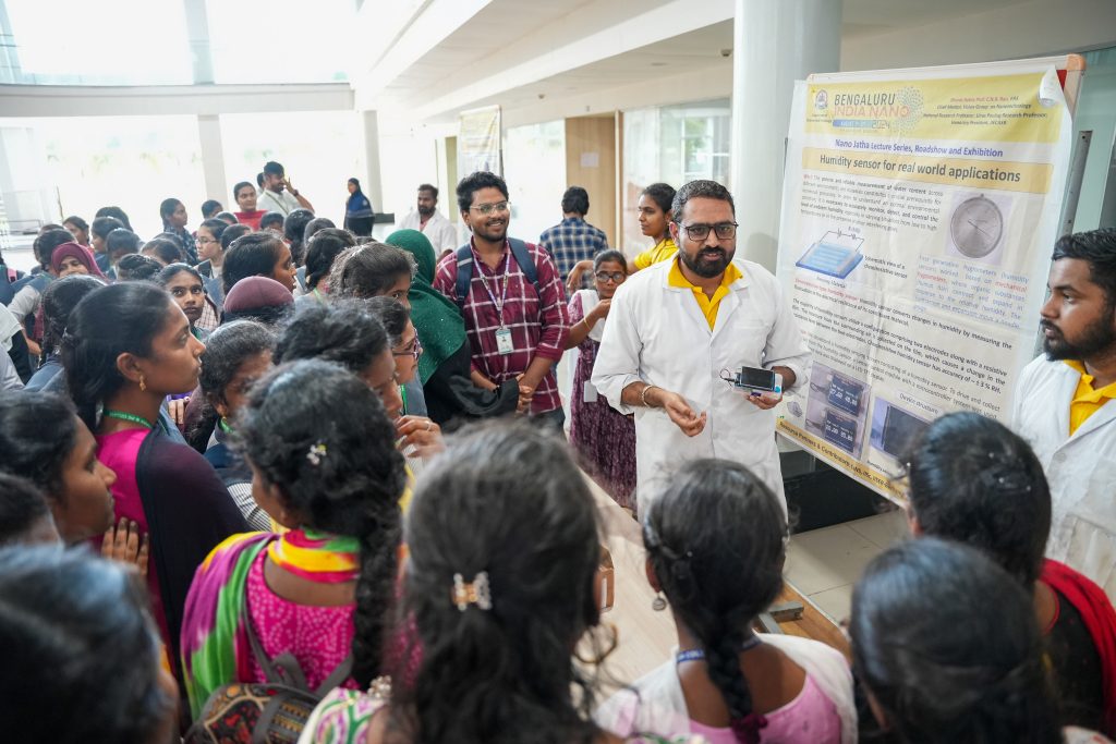
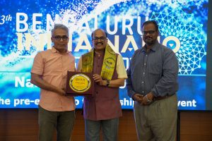
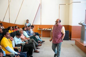
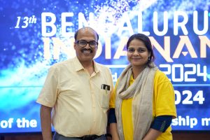
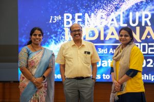
As part of the 13th edition of the Bengaluru India Nano 2024, heralded by Bharat Ratna recipient and renowned chemist Prof. C N R Rao, SRM University-AP hosted “Nano Jatha“, an intensive science outreach programme, catering to educate undergraduate graduates on the emerging trends of nanotechnology, on July 20, 2024. The Nano Jatha programme organised, aimed to raise awareness on nanoscience and technology through technical presentations by expert scientists and a distinctive live experiment demonstration of nano kits focused on showcasing nanoscience ideas.
The event featured two expert talks by eminent dignitaries. Prof. B L V Prasad, Director-Centre for Nano and Soft Matter Sciences (CeNS), Department of Science and Technology, Govt. of India, also serving as the Nodal Officer for organising Nano Jatha events, delivered a session on the introduction to nanoscience and technology. “Nanoscience and technology are often foretold as the technology of the future. This multidimensional technology will revolutionise our understanding of every natural phenomenon and every aspect of human life,” remarked Prof. Prasad in his session.
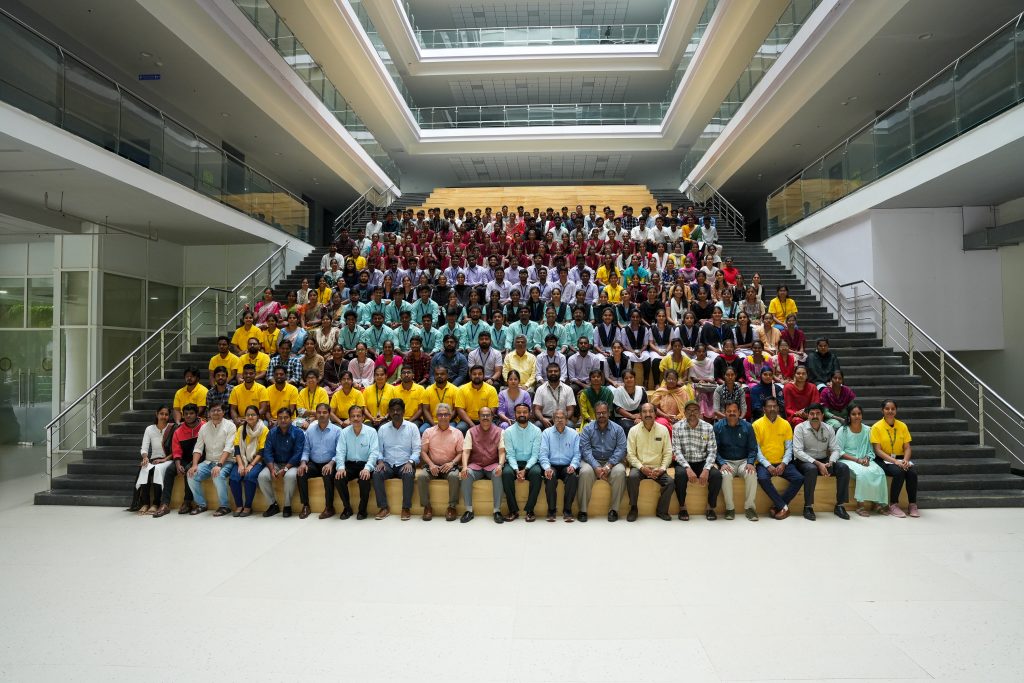
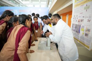
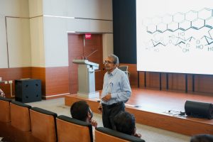
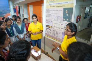
Prof. C P Rao, Senior Professor at the Department of Chemistry, presented the second expert talk on the applications of nanomaterials. The session delved into the properties of covalent molecules and its assemblage leading to cutting-edge technology. The programme also featured an exhibition were experiments on Gold nanoparticle; Galvanization reaction between metals; Piezoelectric pavement for futuristic applications; Humidity sensors for real-world applications and many more were displayed.
Prof. C V Tomy, Dean-School of Engineering & Sciences and Dr Pardha Saradhi Maram, Head-Department of Chemistry, emphasised that the Nano Jatha exemplified the university’s commitment to hands-on learning in science, specifically nanotechnology.They commented that the Department of Chemistry is dedicated to fostering scientific knowledge and igniting passion for chemistry among students and educators alike and will continue to organise events like Nano Jatha, conferences, workshops, and Faculty Development Programmes to achieve the same.
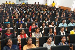
Over 300 students from 7 regional colleges in Andhra Pradesh participated in the programme, displaying their zeal in the discussions and nano kit demonstrations. The event was well executed benefitting the student community significantly in understanding various emerging fields in science and technology.
- Published in Chemistry-news, Departmental News, News
MOU with ASPIRE BioNEST, UoH for Augmenting Innovation and Incubation
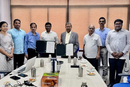
SRM University-AP signs an MOU with the Association for Scientific Pursuits in Innovative Research BioNEST (ASPIRE BioNEST) of the University of Hyderabad, facilitating a dynamic transformation in the innovation and entrepreneurial ecosystem of the institute. Prof. S Rajagopal, Director ASPIRE BioNEST and Dr R Premkumar, Registrar, SRM University-AP signed the MOU in the presence of Dr Anil Kondreddy, COO, ASPIRE BioNEST, Prof. Jayaseelan Murugaiyan, Associate Dean-Sciences, SRM University-AP and Dr Pitchaiah Cherukuri, Assistant Professor, SRM University-AP.
The agreement will ensure guidance and support from ASPIRE BioNEST in establishing, operating and maintaining the best innovation and incubation practices at the SRM AP incubation centres. ASPIRE BioNEST will also provide support in selection of incubates/start-ups, finalising facilities/designs, procurement of instruments and help in formulating guidelines and policies for operating incubation centres at the university.
The MOU is a significant milestone for the young innovators and venturers at SRM AP as ASPIRE BioNEST will furnish internship opportunities with incubatees and startups at ASPIRE, mentor support for startups, collaboration in applying for grant proposals and raising funds, and training and skill development programmes.
Vice Chancellor, Prof. Manoj K Arora expressed his ardour on the collaboration. He stated that “ASPIRE BioNEST is one of the Best Bio-incubator where most of the innovative research is translated into technologies. As an institute that prioritise innovation and entrepreneurship, this MOU will stimulate and enrich SRM University-AP’s entrepreneurial culture, helping us to become one of the preferred incubation and innovation centres in Andhra Pradesh.”
ASPIRE BioNEST of the University of Hyderabad is a deep-tech life sciences incubator established in 2018 with the support of BIRAC, Government of India and ASPIRE, a section 8 non-profit company established by University of Hyderabad. One of the key objectives of ASPIRE BioNEST is to provide support and guidance, including technological, professional and collaborative inputs to help other incubation centres raise their entrepreneurial culture. With the agreement, both SRM University-AP and ASPIRE BioNEST have undertaken to synergistically support each other in the larger interest of innovation and entrepreneurship.
Exploring Wire Arc Additive Manufacturing
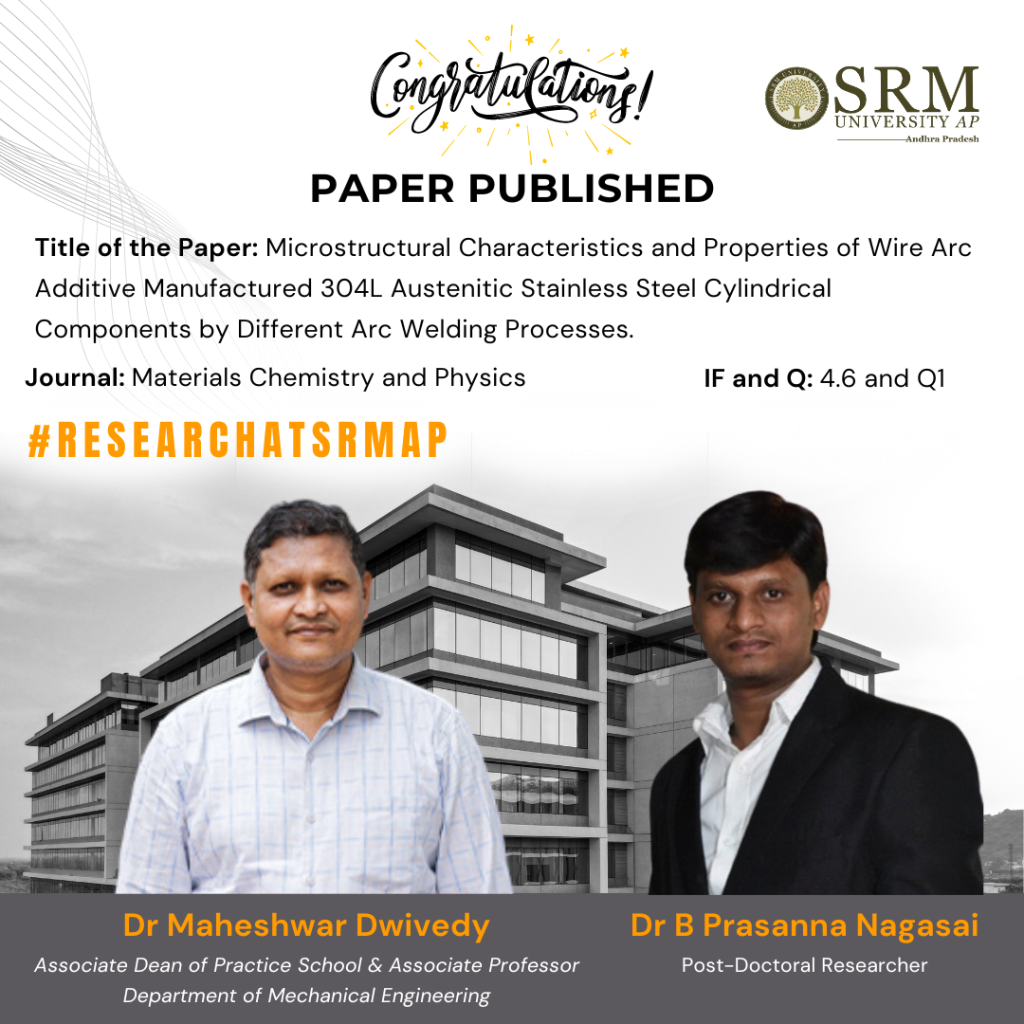
Wire Arc Additive Manufacturing (WAAM) is revolutionizing how we make metal components, especially when it comes to materials like 304L austenitic stainless steel—a popular choice in industries such as aerospace, automotive, and healthcare due to its durability and corrosion resistance. The research paper titled “Microstructural Characteristics and Properties of Wire Arc Additive Manufactured 304L Austenitic Stainless Steel Cylindrical Components by Different Arc Welding Processes” published by Dr Maheswar Dwivedy, Associate Professor, Department of Mechanical Engineering and his post-doctoral scholar Dr B Prasanna Nagasai explores this innovative manufacturing method in detail, focusing on how different welding techniques affect the end product.
Overall, this research indicates that WAAM, with its different welding techniques, can produce 304L stainless steel cylinders that potentially outperform those made by conventional forging, both in terms of material efficiency and mechanical properties. Such findings are significant as they point towards more sustainable and cost-effective manufacturing methods that do not sacrifice quality.
Abstract
Wire arc additive manufacturing (WAAM) is an advanced additive manufacturing (AM) technology that offers low cost and high deposition rates, making it suitable for building large metal parts for structural engineering applications. However, various welding procedures result in differing heat inputs and repetitive heating treatments throughout the deposition process, which can affect the microstructural and mechanical characteristics of the parts. In the current study, cylindrical parts made of 304L austenitic stainless steel (ASS) were manufactured using the WAAM technique, employing both gas metal arc welding (GMAW) and cold metal transfer (CMT) processes. This study explores the correlation between WAAM techniques and their effects on the bead geometry, microstructure and mechanical properties. The paper presents detailed analyses of the microstructure using techniques such as optical microscopy, scanning electron microscopy (SEM), energy-dispersive X-ray spectroscopy (EDS) and X-ray diffraction (XRD). The research findings suggest that the choice of arc welding process significantly affects the grain size, phase distribution, and defect formation within the 304L stainless steel, thereby influencing the mechanical properties and overall performance of the manufactured components. The WAAM-processed 304L ASS cylinders showed better performance compared to those manufactured using traditional industrial forging standards, indicating that WAAM-processed 304L ASS cylinders are suitable for industrial applications. This comprehensive evaluation provides insights into optimising welding processes for enhanced quality and performance of stainless steel cylindrical parts.
Highlights of the research
- Controlling heterogeneous microstructures in WAAM-processed 304L stainless steel is challenging.
- GMAW vs. CMT impacts on 304L ASS microstructure analysed.
- The upward growth of coarse austenite/ferrite morphologies is controlled by the wire retraction mechanism.
- CMT produced finer dendrites and more ferrite morphologies.
- WAAM 304L ASS components outperformed the wrought 304L ASS and forged 304L ASS.

Practical implementation/Social implications of the research
The practical implementation of Wire Arc Additive Manufacturing (WAAM) for 304L austenitic stainless steel could revolutionise multiple industries, including aerospace, automotive, medical devices, maritime, and energy, by allowing the production of complex, custom, and durable components with greater efficiency and reduced material waste. This shift not only promises economic benefits like cost reduction and job creation in advanced manufacturing sectors but also carries significant environmental advantages by minimising waste and the carbon footprint associated with traditional manufacturing processes. Furthermore, the technology enhances supply chain resilience by enabling local, on-demand production, which could be crucial during global disruptions. Socially, WAAM could increase access to customised medical aids in low-income regions, fostering greater equality. The adoption of WAAM thus holds the potential to impact manufacturing practices profoundly, driving innovation, sustainability, and inclusivity across various sectors.
Collaborations
Dr V Balasubramanian, Professor & Director, Centre for Materials Joining & Research (CEMAJOR), Annamalai University, Tamilnadu.
In the future, the research team plan to focus on developing Functionally Graded Materials (FGMs) of nickel and stainless steel using Wire Arc Additive Manufacturing (WAAM). This research will aim to leverage the unique properties of each metal to create components with tailored functional performance for demanding applications. Key challenges will include optimising material interfaces, controlling deposition processes, and ensuring structural integrity.
- Published in Departmental News, Mechanical Engineering NEWS, News, Research News
“Destination Japan”- An Indo-Japanese Alliance for International Recruitment of SRM AP Graduates
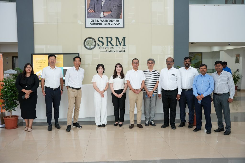
SRM University-AP, with its uniquely curated “Destination Japan” program for its highly skilled Engineering & Non-engineering Students, is an initiative by the university to address the growing demand for human resources in Japan. The ‘Destination Japan’ program provides well-equipped engineers with valuable industry skills and well acquainted with Japanese culture. Under the programme, students are trained in the Japanese language, Japanese traditions, and work culture from the first year onwards, which helps them easily assimilate into the country’s workforce. The initiative also welcomes reputed companies from Japan to directly hire skilled engineering graduates from core engineering fields to enhance their manpower.
SRM University–AP has also signed MOUs with multiple universities in Japan for faculty & student exchange programs, collaborative R&D projects, Hi-tech & innovative labs and other academic initiatives complementing the “ Destination Japan “ program.
To further enhance this mutual alliance, the Director of Corporate Relations & Career Services of SRM AP, Dr Vivekanandan M S, has visited prospective companies and industries in Hamamatsu, Japan, during which he presented the stellar record of engineering graduates being nurtured at the varsity and the possible partnership for recruitment and employment.
SRM University-AP has also signed an agreement with the Shizuoka Government to foster Indo-Japanese academic and recruitment partnerships. These partnerships enable internships in Japanese organisations, admissions to universities for higher studies, and good career placement opportunities for their students in Japan.
Under the “Destination Japan” program, direct campus recruitment has begun with the visit of recruitment teams from two reputed Japanese companies, Forum Engineering Inc. and CRESCO Ltd., to hire proficient engineering graduates. This is a remarkable accomplishment for the university to ensure international placements for its students.
A recruitment team of four from CRESCO Ltd, including the Managing Director, and a team of two from Forum Engineering Inc. visited the university campus. The team included engineers, HR Executives and other professionals.
Many more Japanese companies are lined up for campus visits & recruitment in the coming months.
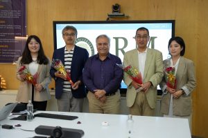
In an interaction with the recruitment teams from Japan, Mr Satoshi Iwami, MD of CRESCO, remarked, “As we are facing a shortage of IT engineers not only in our company but all over Japan, and with the SRM AP harbouring excellent IT engineers, we decided that an alliance would greatly benefit both parties.”
Ms Saho Funahashi, UI/UX Designer at CRESCO, said, “The students’ Japanese skills have impressed me. SRM University-AP has helped students understand the practical way of studying engineering through its impressive resources. This would greatly benefit them in a techno-driven country like Japan.”
Mr Mitsutaka Sekino, Operating Officer at Forum Engineering and Director of Cognavi India stated, “Due to the population crisis, the Japanese economy is getting weaker, but we believe hiring an able workforce from SRM AP to Japan will help improve the economy. We have come to hire excellent students from the university, and I’m greatly impressed by their proficiency in Japanese and their work attitude.”
Mr Masahiro Koizumi, Senior Executive Officer at Forum Engineering and Managing Director of Cognavi India, opined, “We, from Forum Engineering, have come here with the intention of recruiting high-skilled engineers. Furthermore, the clients of Forum Engineering, the manufacturers of electrical and mechanical equipment in Japan, have been facing a shortage of engineers. They desire Indian students to come to Japan and help resolve the problem.”
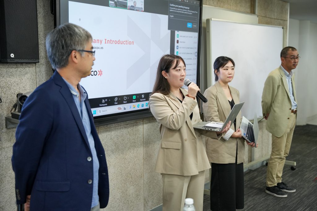
This program is guided and driven by SRM Global Consulting Private Limited, a consulting company of SRM Group established in Japan. Speaking on this, Mr Sankar Karunanidhi, Country Manager, SRM Global Consulting, mentioned, “SRM Group has had a long-standing relationship with Japan for over 25 years. This association has helped us design this unique program and training for our university students”.
This flagship initiative by SRM University-AP is helping Japan alleviate its labour shortage in various industries. Highly skilled graduates from India can get lucrative placements in Japan, ensuring a good work-life balance and career growth opportunities. SRM University–AP, continuing its success of placing students in Japan with the dedicated program and the team behind Destination Japan, envisions placing a minimum of 120 Highly Skilled students in Japan year-on-year.
Vice Chancellor of SRM University-AP, Prof. Manoj K Arora, said this remarkable venture by the two parties would enrich the student’s academic experience, moulding them into global citizens with exceptional industry acumen. “We have established a prolific alliance with Japan. We plan to extend our collaborations to place our students in Taiwan, Canada, Germany and other European countries,” stated the head of the institution.
The continuous dedication and support from the team’s leading both nations guarantee prospective Indian graduates a once-in-a-lifetime opportunity to secure their dream careers in Japan.
- Published in CR&CS, CR&CS NEWS, Departmental News, News
Developing Biosensors using Photonic Crystal Fibres and Surface Plasmon Resonance (SPR)
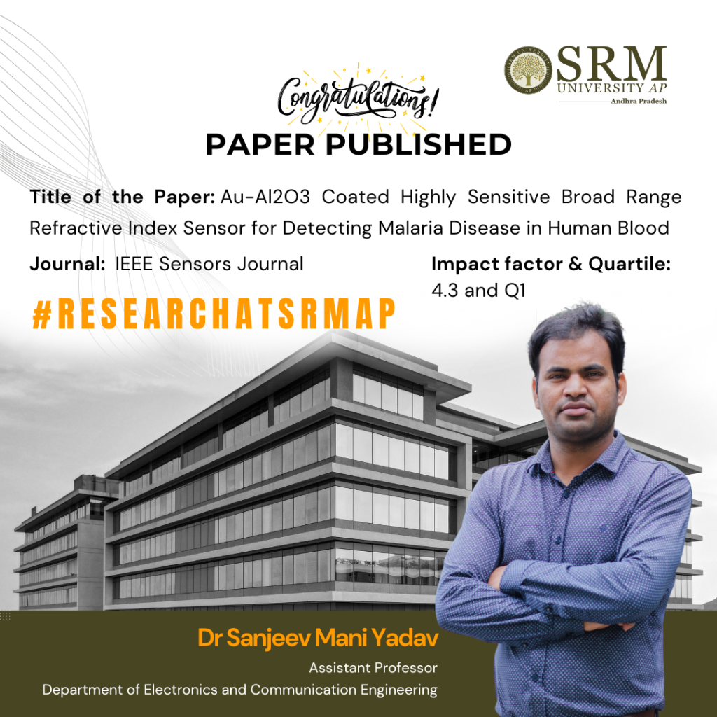
Dr Sanjeev Mani Yadav, Assistant Professor from the Department of Electronics and Communication Engineering, has published a cutting-edge research paper titled “Au-Al2O3 Coated Highly Sensitive Broad Range Refractive Index Sensor for Detecting Malaria Disease in Human Blood” in the IEEE Sensors Journal with an impact factor of 4.3. This research focuses on developing a highly sensitive biosensor using photonic crystal fibres and a technique called surface plasmon resonance (SPR) to detect changes in the refractive index, which is how much light bends when it enters a material. This biosensor can also detect malaria in the human body.
Abstract
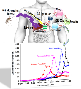
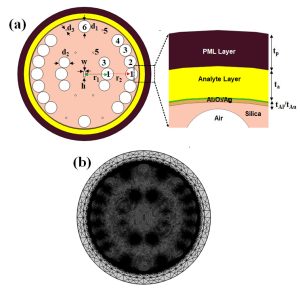
The paper represents the photonic crystal fibre-based surface plasmon resonance (SPR) biosensor for broad-range refractive index sensors along with the detection of malaria disease in the human body. α-Al2O3-Au dielectric-metal interface has been proposed to stimulate the free electron on the metal surface via evanescent to result in an SPR phenomenon. The proposed sensor shows a sufficient shift in resonance wavelength for the change in external RI from 1.32 to 1.40 for an optimised Al2O3/Au thickness of 50nm/12nm. The broad-range sensing applicability of the designed sensor shows a maximum sensitivity of 6000 nm/RIU when the external RI changes from 1.38 to 1.40. The detection accuracy of the designed sensor is reported to be 1.66×10⁻⁵ (RIU) and reported compatible in comparison to broad RI sensors. The proposed SPR sensor has been utilised to sense the malaria diseases in the human body by filling infected RBC samples on the dielectric-metal surface. The proposed study aids in detecting various stages of malaria-infected RBCs, including the Ring phase, Trophozoite phase, and Schizont phase, by measuring the shift in resonance wavelength. The sensor’s wavelength sensitivity varies across the phases: 5714.28 nm/RIU for the Ring phase, 5263.15 nm/RIU for the Trophozoite phase, and 5931 nm/RIU for the Schizont phase. The sensor exhibits the highest reported sensitivity among other biological sensors in this category. The proposed sensor fulfils all the requirements for a diagnosis of early malaria disease in the human body, along with its high sensitivity, low detection limit, and capability of sensing broad RI.
How does the sensor work?
1. Biosensor Basics: The sensor uses a combination of a special crystal fibre and a metal surface (a mix of aluminium oxide and gold) to create a reaction when light hits it. This reaction is called SPR and it helps in detecting tiny changes.
2. Detecting Changes: When the external refractive index (a measure of how light bends in a substance) changes, the sensor detects this by a shift in the wavelength (colour) of the light. The study found that the sensor is very sensitive to changes in the refractive index between 1.32 and 1.40.
3. Sensitivity: The sensor is incredibly sensitive, with a maximum sensitivity of 6000 nm/RIU (nanometres per refractive index unit). This means it can detect very small changes very accurately.
4. Malaria Detection: The sensor can also detect malaria by analysing infected red blood cells. Different stages of malaria infection (Ring, Trophozoite, and Schizont) cause different shifts in the wavelength, which the sensor can measure. The sensor’s sensitivity varies slightly with each stage but is consistently high.
5. High Performance: This sensor is reported to have the highest sensitivity compared to other similar sensors and meets all the requirements for early malaria diagnosis due to its high sensitivity, low detection limit, and ability to detect a wide range of refractive indices.
In essence, this sensor is a powerful tool for detecting both refractive index changes and malaria in the human body with high accuracy and sensitivity.
Practical implementation/Social implications of the research
The photonic crystal fibre-based SPR biosensor represents a significant advancement in medical diagnostics with wide-ranging practical applications and social implications. Its high sensitivity and accuracy in detecting malaria and potentially other diseases can lead to better health outcomes, economic benefits, and improved access to healthcare, particularly in regions that need it the most.
Dr Sanjeev Mani Yadav acknowledges Dr Amritanshu Pandey, Electronics Engineering Department, IIT (BHU) Varanasi, for his continuous support and guidance throughout this research.
- Published in Departmental News, ECE NEWS, News, Research News
A System for Visually Impaired Navigation
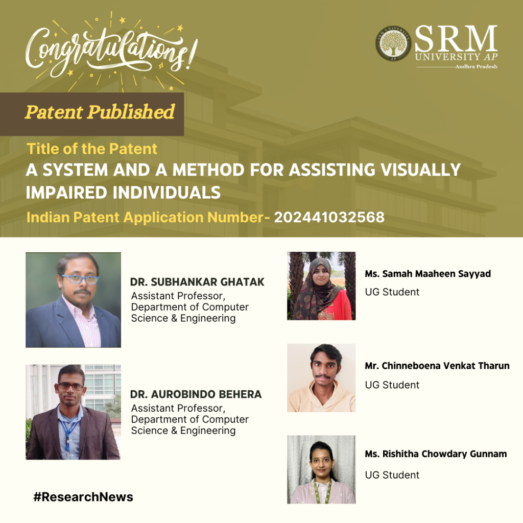
A dedicated team of researchers and professors have developed an innovative patent titled “System and a Method for Assisting Visually Impaired Individuals” that uses cutting-edge technology to significantly improve the navigation experience for visually impaired individuals, fostering greater independence and safety.
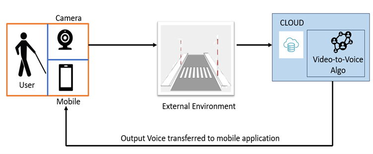
The team, comprising Dr Subhankar Ghatak and Dr Aurobindo Behera, Assistant Professors from the Department of Computer Science and Engineering, and students Ms Samah Maaheen Sayyad, Mr Chinneboena Venkat Tharun, and Ms Rishitha Chowdary Gunnam, has designed a system that transforms real-time visual data into vocals via a mobile app. It will utilise wearable cameras, cloud processing, computer vision, and deep learning algorithms. Their solution captures visual information and processes it on the cloud, delivering relevant auditory prompts to users.
Abstract
This patent proposes a novel solution entitled, “System and a method for assisting visually impaired individuals aimed at easing navigation for visually impaired individuals. It integrates cloud technology, computer vision algorithms, and Deep Learning Algorithms to convert real-time visual data into vocal cues delivered through a mobile app. The system
employs wearable cameras to capture visual information, processes it on the cloud, and deliver relevant auditory prompts to aid navigation, enhancing spatial awareness and safety for visually impaired users.
Practical implementation/Social implications of the research
The practical implementation of our research involves several key components. Firstly, we need to develop or optimise wearable camera devices that are comfortable and subtle for visually impaired individuals to wear. These cameras should be capable of capturing high-quality real-time visual data. Secondly, we require a robust cloud infrastructure capable of processing this data quickly and efficiently using advanced computer vision algorithms and Deep Learning Algorithms. Lastly, we need to design and develop a user-friendly mobile application that delivers the processed visual information as vocal cues in real-time. This application should be intuitive, customisable, and accessible to visually impaired users.
The social implications of implementing this research are significant. By providing visually impaired individuals with a reliable and efficient navigation aid, we can greatly enhance their independence and quality of life. Navigating city environments can be challenging and hazardous for the visually impaired, leading to increased dependency and reduced mobility. Our solution aims to mitigate these challenges by empowering users to navigate confidently and autonomously. This fosters a more inclusive society where individuals with visual impairments can participate actively in urban mobility, employment, and social activities.
In the future, we plan to further enhance and refine our technology to better serve the needs of visually impaired individuals. This includes improving the accuracy and reliability of object recognition and scene understanding algorithms to provide more detailed and contextually relevant vocal cues. Additionally, we aim to explore novel sensor technologies and integration methods to expand the capabilities of our system, such as incorporating haptic feedback for enhanced spatial awareness.
Furthermore, we intend to conduct extensive user testing and feedback sessions to iteratively improve the usability and effectiveness of our solution. This user-centric approach will ensure that our technology meets the diverse needs and preferences of visually impaired users in various real-world scenarios.
Moreover, we are committed to collaborating with stakeholders, including advocacy groups, healthcare professionals, and technology companies, to promote the adoption and dissemination of our technology on a larger scale. By fostering partnerships and engaging with the community, we can maximize the positive impact of our research on the lives of visually impaired individuals worldwide.
- Published in CSE NEWS, Departmental News, News, Research News
Significant Advancement in Analytical Detection of NFZ by the Department of Chemistry and RARE Lab
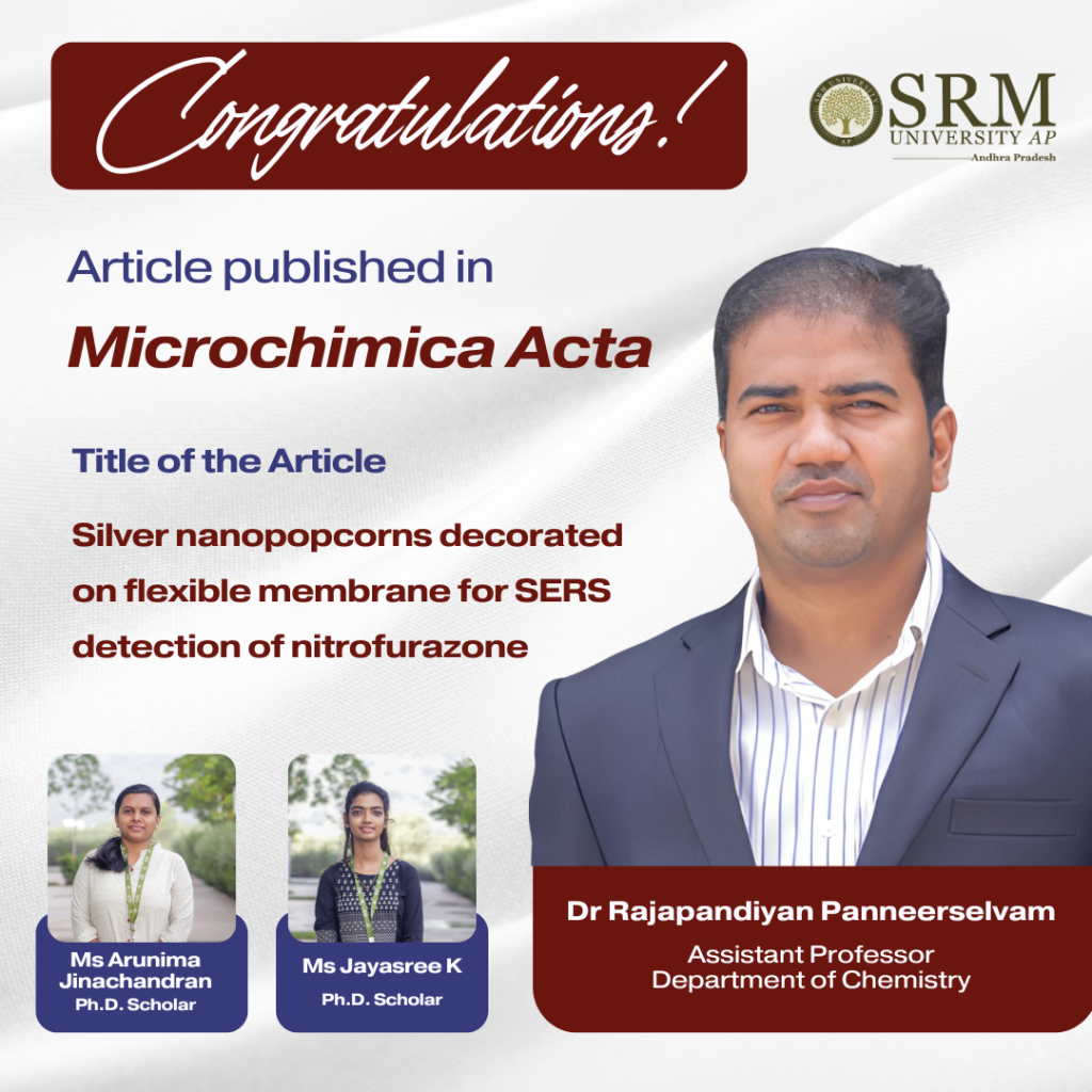
The Department of Chemistry and RARE Lab are excited to announce a groundbreaking advancement in the field of analytical detection. Researchers Dr Rajapandiyan Panneerselvan, Asst. Professor and Ph.D scholars, Ms Arunima Jinachandran and Ms Jayasree Kumar have developed a novel method for detecting nitrofurazone (NFZ) using three-dimensional silver nanopopcorns (Ag NPCs) on a flexible polycarbonate membrane (PCM) in their paper “Silver nanopopcorns decorated on flexible membrane for SERS detection of nitrofurazone” published in Microchimica Acta. This innovative technique leverages the power of surface-enhanced Raman spectroscopy (SERS) to provide a highly sensitive and practical solution for detecting NFZ on various surfaces, including fish.
Nitrofurazone (NFZ) is an antibiotic commonly used in veterinary medicine that poses significant health risks if residues enter the food chain. Despite regulatory bans, its illegal use continues, necessitating highly sensitive detection methods. While effective, traditional methods such as high-performance liquid chromatography and mass spectrometry are often costly and labor-intensive. The new SERS-based method offers a more efficient and straightforward alternative.
Abstract
The synthesis of three-dimensional silver nanopopcorns (Ag NPCs) onto a flexible polycarbonate membrane (PCM) for the detection of nitrofurazone (NFZ) on fish surfaces by surface-enhanced Raman spectroscopy (SERS) is presented. The proposed flexible Ag-NPCs/PCM SERS substrate exhibits significant Raman signal intensity enhancement with a measured enhancement factor of 2.36 × 10^6. This enhancement is primarily attributed to the hotspots created on Ag NPCs, which include numerous nanoscale protrusions and internal crevices distributed across the surface. The detection of NFZ using this flexible SERS substrate demonstrates a low limit of detection (LOD) of 3.7 × 10^−9 M and uniform, reproducible Raman signal intensities with a relative standard deviation below 8.34%. The substrate also exhibits excellent stability, retaining 70% of its efficacy even after 10 days of storage. Notably, the practical detection of NFZ in tap water, honey water, and fish surfaces achieves LOD values of 1.35 × 10^−8 M, 5.76 × 10^−7 M, and 3.61 × 10^−8 M, respectively, highlighting its effectiveness across different sample types. The developed Ag-NPCs/PCM SERS substrate presents promising potential for the sensitive SERS detection of toxic substances in real-world samples.
Methodology
The synthesis involves creating silver nanopopcorns on a flexible polycarbonate membrane using a simple chemical method. The resulting Ag NPCs exhibit high surface roughness with numerous nanoscale features that enhance the Raman signal. This flexible substrate can easily collect samples from irregular surfaces without requiring extensive preparation.
This SERS substrate can detect NFZ in various real-world samples, including:
- Tap water
- Honey water
- Fish surfaces
The method’s sensitivity and ease of use make it a promising tool for ensuring food safety and monitoring environmental contaminants.
The Department believes this development will significantly impact public health by providing a reliable and accessible method for detecting harmful substances in the food chain.
- Published in Chemistry-news, Departmental News, News, Research News
Innovative System for Detection and Classification of Manufacturing Defects in PCB
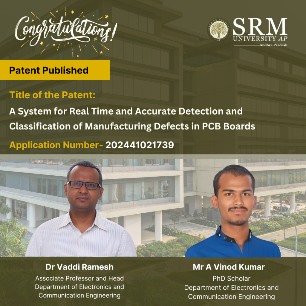
Dr Ramesh Vaddi, Associate Professor & Head of the Department of Electronics and Communication Engineering, along with his PhD Scholar Mr A Vinod Kumar has developed a new system for real-time and accurate detection and classification of manufacturing defects in Printed Circuit Boards (PCBs). This groundbreaking invention has been filed and published with Application Number: 202441021739 in the Patent Office Journal.
Abstract
This study presents a new system for real-time detection and classification of defects in Printed Circuit Boards (PCBs), which are critical in electronic products and systems. It employs an efficient model with pre-trained weights to detect defects for enhanced quality control. The model is initially trained and fine-tuned on a computer and then deployed on a compact computing board. For real-time imaging, a high-definition USB camera is connected to the system, allowing direct defect identification without the need for external devices. The output is shown on a monitor, with the PCB image featuring clearly labelled boxes to indicate the type and location of defects. This method offers a streamlined approach to defect classification, helping to improve the quality control process in electronics manufacturing.
Explanation of the Research in Layperson’s Terms
This research focuses on finding defects in PCBs, which are essential for most electronic devices like computers and phones. The system uses a powerful computer model to quickly identify any defects in real time. The model is trained on a regular computer to recognise normal PCBs and various defects. Once ready, it is transferred to a small, efficient computer board. A camera captures images of the PCBs, and the system analyses these images to identify defects. The results are displayed on a screen, clearly marking where the defects are and what types they are. This helps companies quickly and accurately detect defects in their electronics manufacturing process, saving time, reducing waste, and improving product quality
Practical Implementation/Social Implications of the Research
The practical implementation of this research involves deploying a system for real-time detection and classification of defects in PCBs, essential components in nearly all electronic devices. Using advanced deep learning techniques, the system can quickly identify manufacturing defects early in the production process. This leads to significant improvements in quality control, reduced waste, and lower production costs. By improving quality control in electronics manufacturing, the system helps reduce electronic waste, a significant environmental concern. Early detection of defects also decreases the chances of faulty electronic products reaching consumers, enhancing safety and reducing the need for product recalls. The system’s efficiency and accuracy could lead to more reliable electronics, fostering greater consumer trust in electronic products. This, in turn, encourages companies to invest in higher-quality manufacturing processes, ultimately leading to a more sustainable and responsible electronics industry.
Collaborations
To develop this system, the research team first trained a computer model to recognise defects in PCBs. The training involved feeding the model a large dataset of PCB images, some with defects and some without. The model learned to identify common defects by analysing these examples. Once trained, the model was implemented in a real-time setting and integrated with equipment to inspect PCBs during production. The system used a camera to capture images of each PCB and applied the trained model to analyse these images for defects. Running in real-time, the system could immediately detect issues and alert the manufacturing team, allowing them to correct problems on the spot. This approach improved product quality, reduced the chances of defective electronics reaching consumers, sped up the quality control process, and reduced waste, making the manufacturing process more efficient.
Future Research Plans
The research team has outlined several future plans to enhance and expand their defect detection system for PCBs:
- Model Optimization: Refining the machine learning model to improve accuracy and speed, experimenting with different architectures and training techniques to boost performance.
- Expanded Defect Library: Gathering a more extensive dataset of PCB defects to enable the model to identify a wider range of issues, making the system more versatile for various manufacturing environments.
- Real-World Testing: Testing the system in a broader range of manufacturing settings to ensure robustness and adaptability, understanding performance in diverse scenarios, and fine-tuning for optimal results.
- Integration with Manufacturing Systems: Aiming to integrate the system with other manufacturing processes and technologies for seamless communication between defect detection and other quality control systems, enhancing overall workflow.
- Automation and Robotics: Exploring the use of automation and robotics to streamline the defect detection process, potentially leading to a more automated manufacturing line with reduced human intervention and errors.
- Collaboration and Partnerships: Planning to collaborate with more industry partners and academic institutions to accelerate research and development, gaining valuable insights and resources to advance the system.
- Published in Departmental News, ECE NEWS, News, Research News

