Patent on IoT System for Sensor Data Monitoring and Geo-Storage

Prof. Rupesh Kumar from the Department of Electronics and Communication Engineering and his research cohort, Mr Venkata Naga Sai Kiran Damarla, Mr Prasannakumar Seelam, Ms V L S Tanmay P, and Mr Venkata Ramana Murthy Pondala (BTech ECE students), has published a patent titled “An Integrated Iot System for Sensing, Monitoring, and Geo-Information Storage of Sensor Data” with Application No: 202441065318 for their breakthrough research on developing an intelligent IoT system that can detect environmental changes.
Abstract
This research presents an integrated IoT system designed to monitor environmental conditions and store the corresponding data along with geo-information. The system autonomously collects data from its surroundings, processes it, and stores the information for future retrieval. The system is designed for use in remote monitoring applications where consistent tracking of environmental variables and location data is essential.
Explanation of the Research in Layperson’s Terms
The project aims to create a smart system that can sense changes in its environment—like temperature or humidity—and record those changes alongside its current location and time stamp. The collected data is stored so that it can be retrieved later for analysis, making the system useful in situations like monitoring climate conditions in farming or tracking environmental changes in various locations.
Practical Implementation/Social Implications of Research
The practical implementation of this system spans various fields such as agriculture, environmental management, and logistics. For example, in agriculture, the system can help farmers track environmental changes, allowing them to optimize crop management. Similarly, it can monitor environmental conditions in remote areas, ensuring timely interventions when necessary. The system could also aid in asset tracking, providing both environmental data and the location of critical resources. Its broader social impact lies in its ability to automate data collection, improve accuracy, and reduce human intervention in critical monitoring tasks.

Collaboration
This project was completed with the support and guidance of the Wireless Sensing & Imaging (WSI) Lab. The research team worked closely within the lab to develop the system, utilising the lab’s resources and expertise to achieve the research goals. There were no external collaborations involved in this project.
Prof. Rupesh and his team plan to explore radar design and focus on working with radar technology in their future research. By developing and integrating radar systems, the team aims to enhance IoT applications with advanced sensing capabilities, such as distance measurement, object detection, and environmental monitoring. Their goal is to contribute to more accurate and reliable solutions through the implementation of IoT Integrated Radar technology.
- Published in Departmental News, ECE NEWS, News, Research News
A Grand Book Exhibition Successfully Concludes at SRM AP

The Central Library hosted a highly successful Book Exhibition from November 21 – 23, 2024 in collaboration with Shah Books House (Hyderabad), Shanthi Book House (Chennai), and ISKCON Society (Vijayawada). The exhibition offered a wide range of books covering academic references, research materials, and general interest genres, catering to students, faculty, and staff. Special discounts were available to attendees, making this event an enriching experience for everyone involved.
Our exhibition was inaugurated by Dr Vinayak Kalluri, Dean – Academic Affairs and Prof. C V Tomy, Dean – SEAS in the presence of Vice Chancellor Prof. Manoj K Arora, who praised the exhibition’s ability to promote reading habits and encourage academic curiosity among students and faculty alike. Over 500 attendees, including students, faculty members, and visiting scholars, enthusiastically participated, all of whom explored the rich collection of books on display.
The collaboration with the partnering organisations ensured that the needs of the academic community were met, with resources spanning across disciplines, research interests, and general reading preferences. Many students highlighted the wide variety of books available, extending beyond the core curriculum and including topics catering to their interests and career goals. Faculty members appreciated the opportunity to recommend books for future acquisitions, ensuring the library remains up-to-date with the latest academic trends and resources.
The 2024 Book Exhibition was a resounding success, fostering a deeper connection to reading within the SRM University-AP community. The collaborative efforts of the vendors and ISKCON Society, along with the enthusiastic participation of students and faculty, made this a memorable event. Moving forward, the university plans to expand future exhibitions by incorporating more digital reading resources and hosting guest speakers to enhance the experience further.
- Published in News, University Event
Research on Real-Time Detection and Classification of Defects in PCBAs
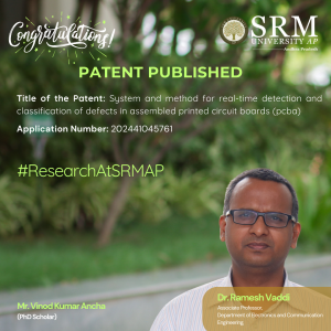
 In today’s fast-paced technological world, ensuring the quality and reliability of electronic devices is essential. Associate Professor Dr Ramesh Vaddi and his research Scholar Mr Vinod Kumar Ancha from the Department of Electrical and Electronics Engineering introduce an innovative system for real-time detection and classification of defects in PCBAs, leveraging advanced machine learning techniques. Their research titled, “System And Method For Real-Time Detection And Classification of Defects in Assembled Printed Circuit Boards (PCBA)” was published in the Patent Journal with Application number 202441045761.
Abstract:
This study presents a new system for real-time detection and classification of defects in Assembled Printed Circuit Boards (PCBAs), which are critical in electronic products and systems. It employs an efficient model with pretrained weights to detect defects for enhanced quality control. The model is initially trained and fine-tuned on a computer, then deployed on a compact computing board. For real-time imaging, a high-definition USB camera is connected to the system, allowing direct defect identification without the need for external devices. The output is shown on a monitor, with the PCBA image featuring clearly labeled boxes to indicate the type and location of defects. This method offers a streamlined approach to defect classification, helping to improve the quality control process in electronics manufacturing.
Explanation of the Research in layperson’s terms:
This research focuses on finding defects or flaws in Assembled Printed Circuit Boards (PCBAs). Which are the “backbone” of most electronic devices, like computers and phones. This system uses a powerful computer model to “look” at these boards and quickly identify any defects, like missing holes, mouse byte, open circuit, short circuit, spur and spurious copper in real-time. The research starts by training this model using a deep learning object detection model on a regular computer, teaching it to recognize what a normal PCBA looks like and what various defects might look like. Once it’s ready, we transfer the model to a small, efficient computer edge board, which does all the processing. A camera is used to capture images of the PCBAs, and the system analyzes these images to find respective defects. The results are displayed on a screen, where it clearly marks where the defects are and what kind of defects they are. Overall, this system helps companies detect defects in their electronics manufacturing process quickly and accurately, which can save time, reduce waste, and improve the quality of their products.
Practical Implementation:
The practical implementation of our research involves deploying a system for real-time detection and classification of defects in Assembled Printed Circuit Boards (PCBAs) a crucial component in nearly all electronic devices. By using advanced Deep learning techniques, our system can quickly identify manufacturing defects, allowing electronics manufacturers to detect the defect early in the production process. This can lead to significant improvements in quality control, reduced waste, and lower production costs. By improving quality control in electronics manufacturing, the system can help reduce electronic waste, which is a significant environmental concern. Early detection of defects also reduces the chances of faulty electronic products reaching consumers, thereby improving safety and reducing the need for product recalls. Additionally, the efficiency and accuracy of our system could lead to more reliable electronics, contributing to greater consumer trust in electronic products. This, in turn, could encourage companies to invest in higher-quality manufacturing processes, ultimately leading to a more sustainable and responsible electronics industry.
Collaborations:
To develop our system, we first trained a computer model to recognize defects in Assembled Printed Circuit Boards (PCBAs). This training process involved feeding the model a large dataset of PCBA images, some with defects and some without. By analyzing these examples, the model learned to identify common defects, like Missing hole, mouse byte, open circuit, short circuit, Spur and Spurious copper. Once the model was trained, we implemented it in a real-time setting. This meant integrating it with equipment that could inspect PCBAs as they were being produced. The system used a camera to capture images of each PCBA and then applied the trained model to analyze those images, checking for any defects. With the model running in real-time, the system could immediately detect issues and alert the manufacturing team, allowing them to correct problems on the spot. This approach helped improve the quality of the final product and reduced the chances of defective electronics reaching consumers. It also sped up the quality control process and reduced waste, making the entire manufacturing process more efficient.
Future Research Plans:
Our future research plans focus on enhancing and expanding our system for defect detection in Assembled Printed Circuit Boards (PCBAs):
Model Optimization: We aim to further refine our machine learning model to improve accuracy and speed. This includes experimenting with different architectures and training techniques to boost performance.
Expanded Defect Library: We plan to gather a more extensive dataset of PCBA defects, allowing our model to identify a wider range of issues. This will make the system more versatile and capable of handling various manufacturing environments.
Real-World Testing: We intend to test our system in a broader range of manufacturing settings to ensure its robustness and adaptability. This will help us understand how it performs in diverse real-world scenarios and how we can fine-tune it for optimal results.
Integration with Manufacturing Systems: Our goal is to integrate our system with other manufacturing processes and technologies. This will allow for seamless communication between defect detection and other quality control systems, enhancing the overall manufacturing workflow.
Automation and Robotics: We’re interested in exploring the use of automation and robotics to streamline the defect detection process. This could lead to a more automated manufacturing line, reducing human intervention and potential errors.
Collaboration and Partnerships: We plan to collaborate with more industry partners and academic institutions to accelerate our research and development. These partnerships will provide valuable insights and resources for advancing our system.
- Published in Departmental News, ECE NEWS, News, Research News
Advancing Next-Gen Networks with MIMO Channel Capacity at 300 GHz

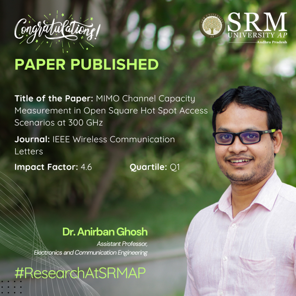
The Department of Electronics and Communication Engineering is pleased to announce the publication of a significant research paper by Dr Anirbhan Ghosh, Assistant Professor, exploring MIMO channel capacity at high frequencies (300 GHz), which holds great potential for beyond 5G and 6G networks. The paper “MIMO Channel Capacity Measurement in Open Square Hot Spot Access Scenarios at 300 GHz” published in the Q1 journal IEEE Wireless Communication Letters, investigates data transmission in three different line-of-sight (LoS) scenarios and contributes to building the next generation of communication networks, which will have a significant positive impact on society by improving connectivity, supporting technological advancements, and promoting economic development.
Abstract
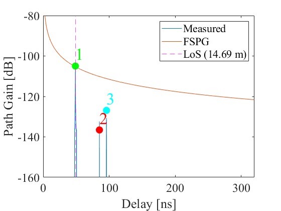
This letter explores the possibility and effectiveness of using multiple communication paths for futuristic outdoor networks, focusing on three scenarios: clear line-of-sight (LoS), partially obstructed line-of-sight (OLoS), and completely blocked line-of-sight (NLoS). A study was conducted at a high frequency of 300 GHz to measure how many useful communication paths are available for transmitting data simultaneously. Based on the results, the average data transmission capacity for these paths was calculated, both with and without the help of passive reflecting surfaces (PRS). The findings show that using multiple antennas significantly boosts the average data capacity, and PRS further enhances this improvement.

Practical Implementation of the Research
The results align with the design of high-frequency, ultra-high-speed, low-latency, reliable communication envisioned for several futuristic applications beyond 5G and 6G Networks.
Collaborations
Prof. Minseok Kim, Professor, Faculty of Engineering, Course of Electrical and Electronics Engineering, Niigata University, Japan.
Dr Ghosh plans to extend his efforts to other communication scenarios for a similar study. He opines that generating appropriate channel models, coverage design, etc., for the explored scenario would also be an exciting study.
- Published in Departmental News, ECE NEWS, News, Research News


