All Management Events
- Prof. Naik Expounds on the Future of Biomedical Imaging November 2, 2023
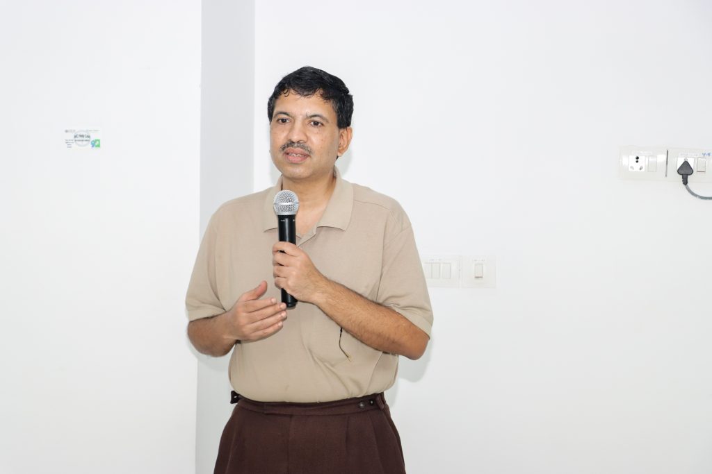
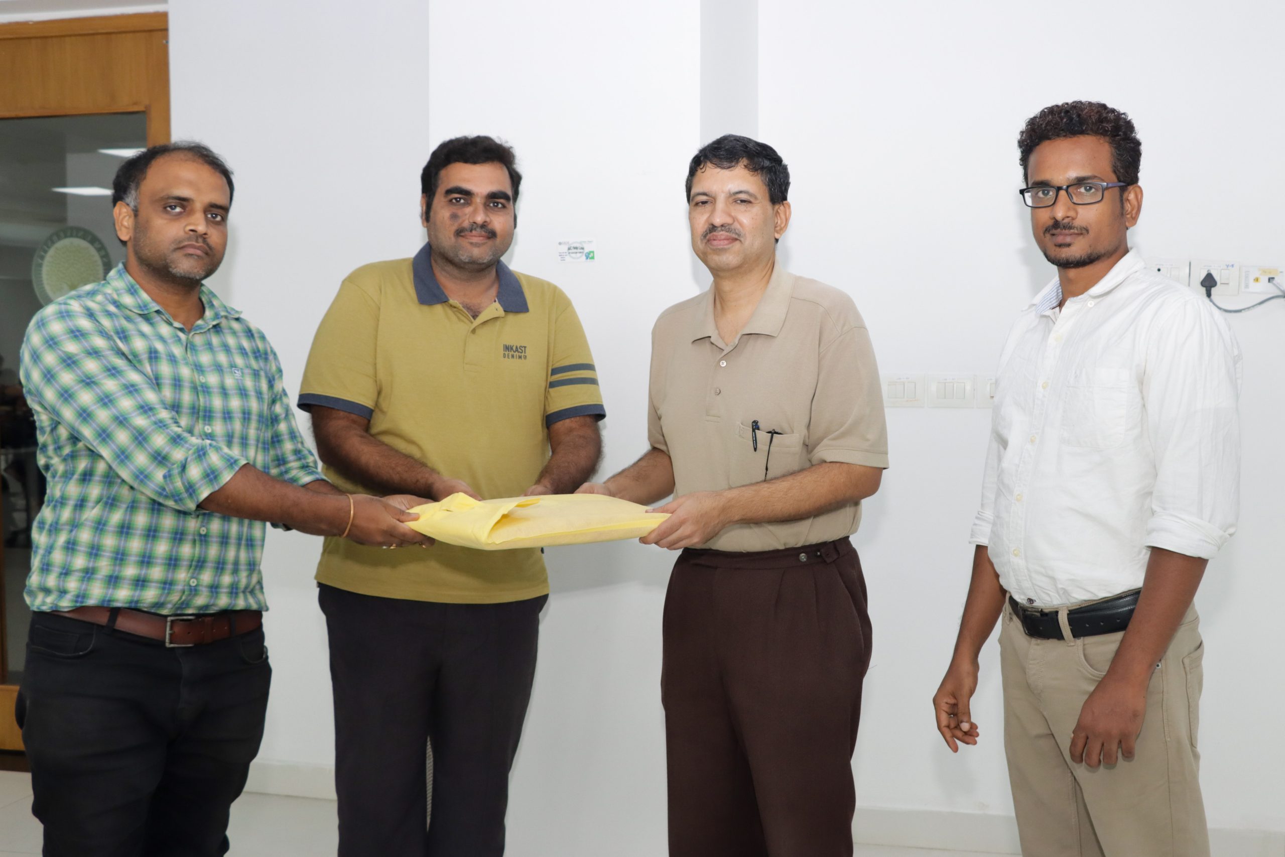
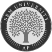
The Department of Electronics and Communication Engineering hosted an Invited Talk on “Dynamic Shape-based Biomedical Tomographic Reconstruction Algorithms” by Prof. Naren Naik, IIT Kanpur on October 30, 2023. Prof. Naren Naik, a well-acclaimed researcher and specialist in tomography reconstruction algorithms discussed extensively on tomographic problem definition and formulation, shape reconstructions, shape-tomography based on radial basis functions (RBF), and the diagnosis of early-stage cancer using tomography. He also explored replacing nuclear medicine modalities with optical fluorescence methods, especially in applications like early cancer detection and metabolic imaging. Additionally, the presentation delved into nonlinear-reconstruction frameworks for fluorescence optical tomography.
Faculty, Research scholars and BTech students from various departments participated in this insightful session. The event was organised by Assistant Professor, Dr V Sateeshkrishna Dhuli of the Department of Electronics and Communication Engineering, SRM University-AP.
Continue reading →

- Dr Pratikanta Mishra November 2, 2023
- SRM University-AP Signed MOU with University of South Florida November 2, 2023
The Hindu
Continue reading →
The Times of India
The New India Express

The Hans India
The Pioneer
Eenadu
Surya

Andhra Prabha
Prajasakthi

Visalaandhra

Vartha

Vartha Prapancham

Arth Prakash

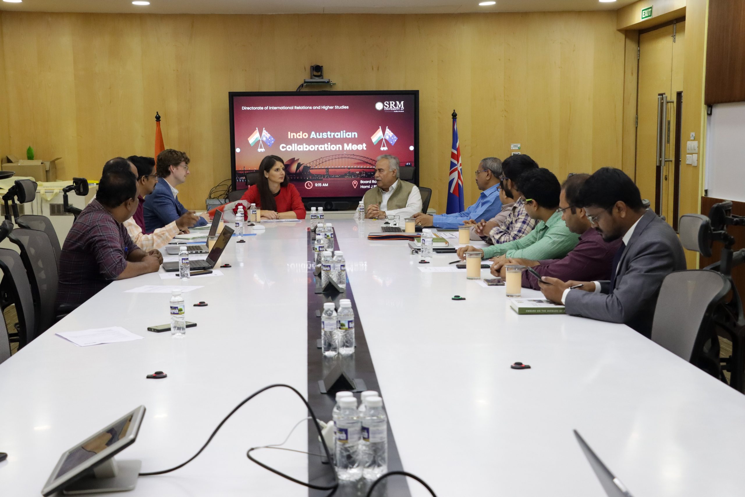
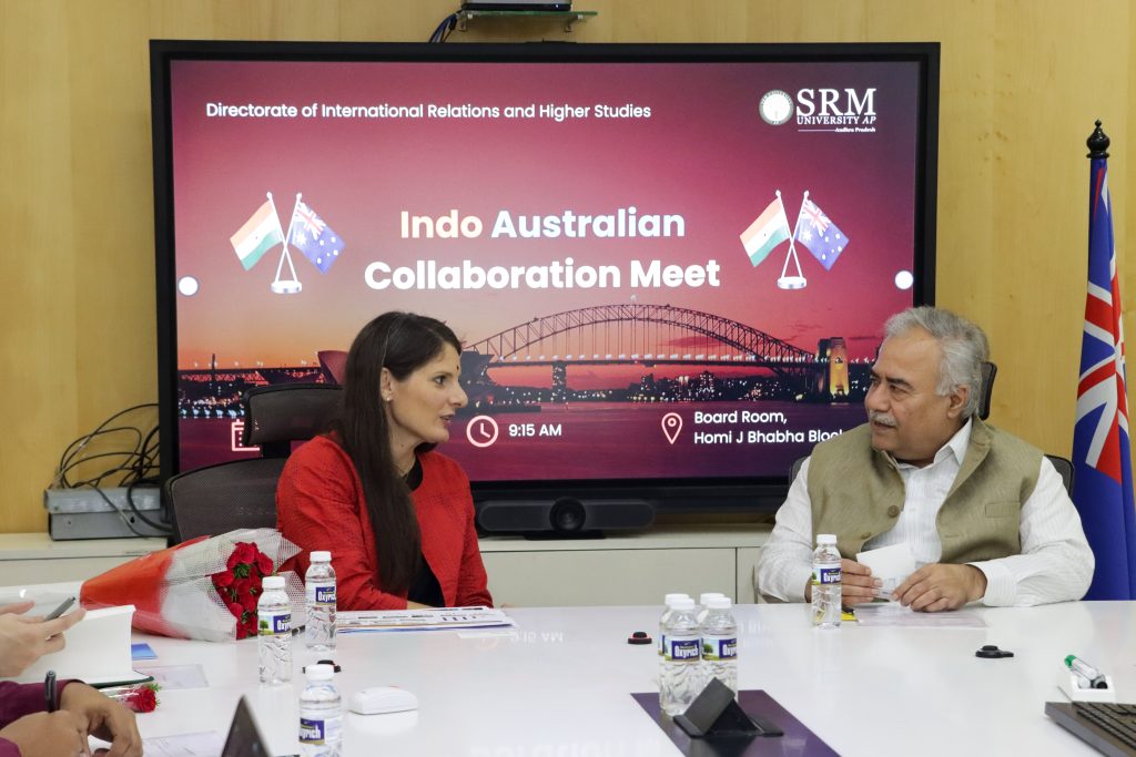
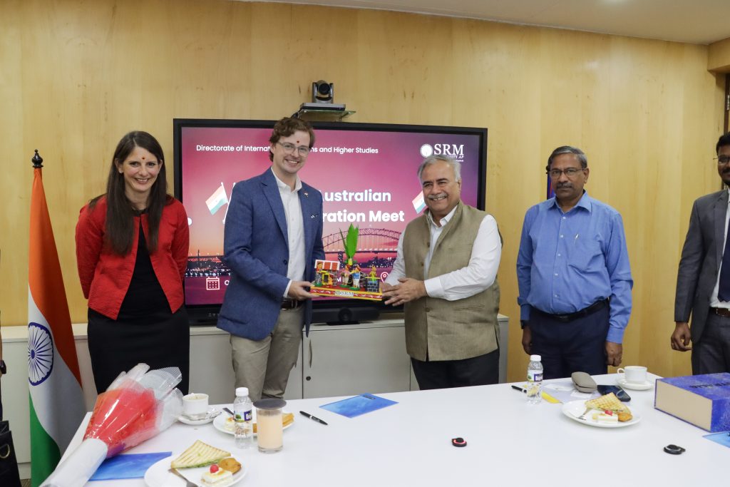
- SRM AP Hosts Australian Delegation for Collaborative Initiatives November 1, 2023
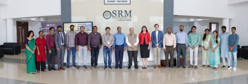
SRM University-AP played host to a dynamic and visionary Indo-Australian Collaboration Meet aimed at fostering academic partnerships and research collaborations between the two nations. The event featured a delegation led by H.E. Sarah Kirle, the Australian Consulate General. It occurred in the esteemed presence of Vice Chancellor Prof. Manoj K Arora and Registrar Dr R. Premkumar.
The Collaboration provided a platform for fruitful discussions and exploring potential collaborative initiatives between educational institutions in India and Australia. The discussions centred around ways to promote the exchange of knowledge, faculty and students, as well as joint research initiatives and cultural programs. Both parties expressed their commitment to developing academic exchange programmes that would allow students and faculty to gain a deeper understanding of each other’s cultures and educational environments. The meeting identified potential research areas where Australian institutions and SRM University-AP could work together to address global challenges and significantly contribute to the respective fields.
The panel featured discussions and brainstorming sessions, with research taking centre stage. The parties deliberated on developing a framework for collaborative research projects, which would encourage knowledge exchange and innovative solutions to global challenges. Discussions revolved around student and faculty exchange programmes, fellowship, and scholarship opportunities that would promote cross-cultural understanding and enrich the educational experience.
The visit served as a significant step in fostering relationships between SRM University-AP and Australian institutions, with the shared goal of promoting global education and research. It will signify a commitment to expanding horizons and offering students a broader and more enriching educational experience.

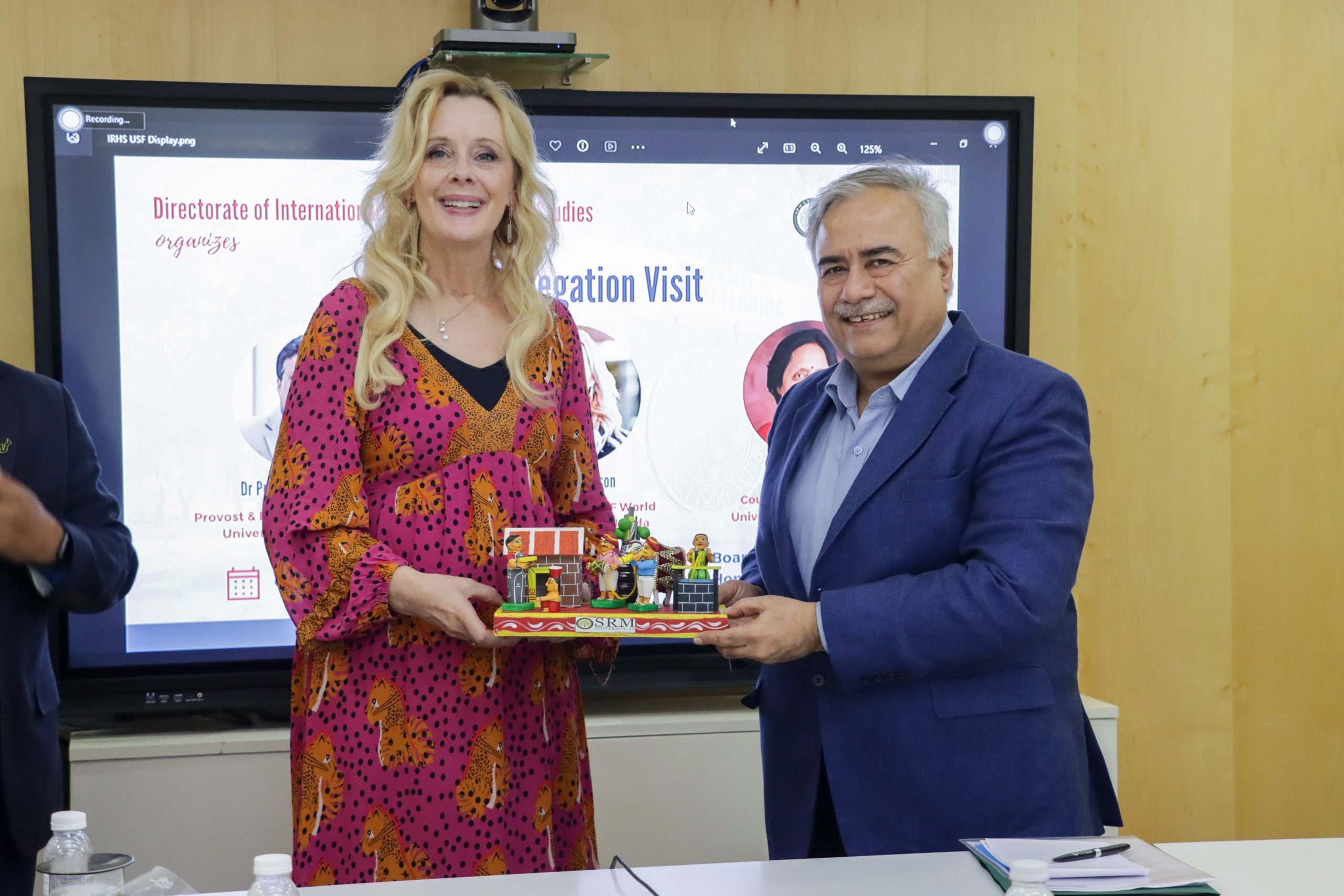
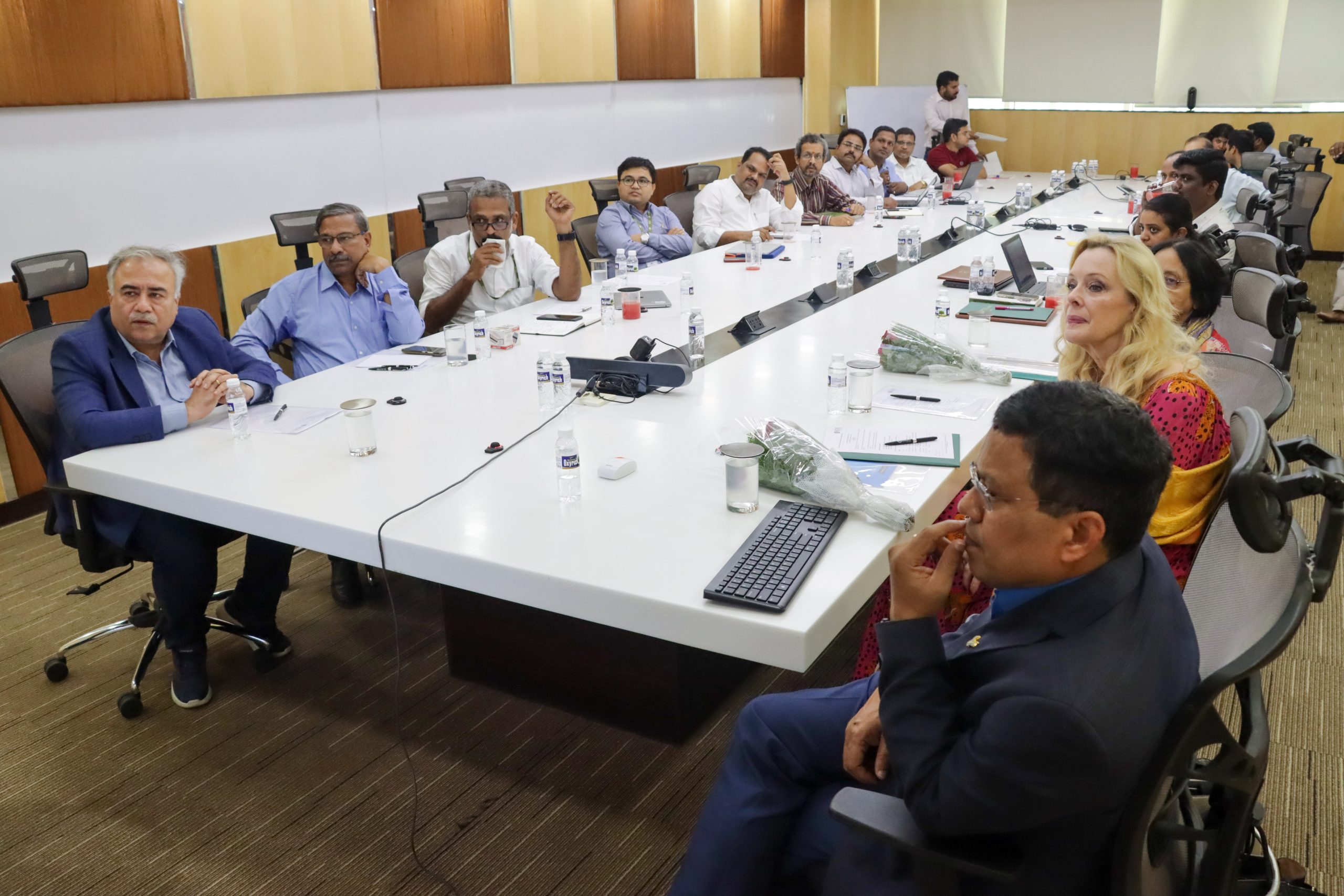
Continue reading → - SRM University-AP Signed MOU with University of South Florida November 1, 2023
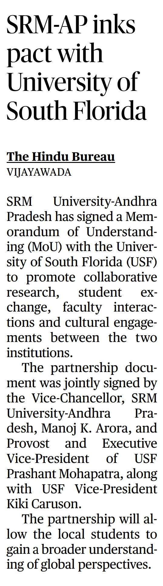
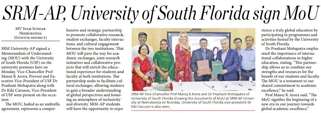
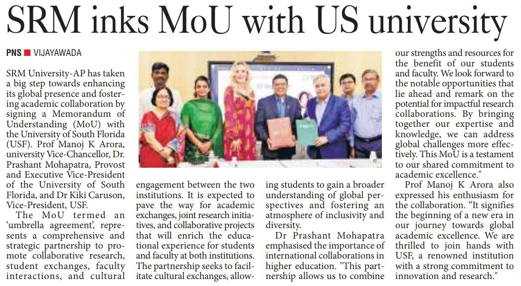
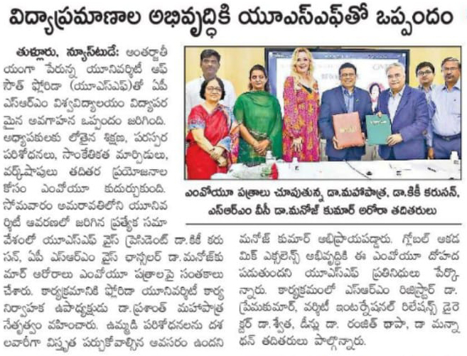
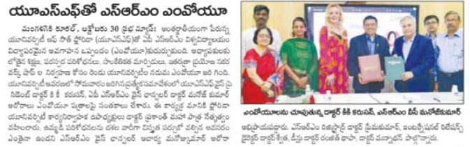
SRM University-AP, Andhra Pradesh, takes a momentous step towards enhancing its global presence and fostering academic collaboration by signing a Memorandum of Understanding (MOU) with the University of South Florida (USF). This historic event took place in the esteemed presence of Prof. Manoj K Arora, Vice Chancellor, SRM University-AP, Dr Prashant Mohapatra, Provost & Executive Vice President of the University of South Florida, along with Dr Kiki Caruson, Vice President, USF.
The MOU hailed as an “umbrella agreement” represents a comprehensive and strategic partnership to promote collaborative research, student exchanges, faculty interactions, and cultural engagement between the two institutions. This MOU will pave the way for academic exchanges, joint research initiatives, and collaborative projects that will enrich the educational experience for students and faculty at both institutions. The partnership seeks to facilitate cultural exchanges, allowing students to gain a broader understanding of global perspectives and fostering an atmosphere of inclusivity and diversity. SRM University-AP students will have the opportunity to experience a truly global education by participating in programs and activities hosted by the University of South Florida. Joint research projects will allow both institutions to tackle complex global challenges and significantly contribute to their respective academic fields.
Dr Prashant Mohapatra emphasised the importance of international collaborations in higher education, stating, “This partnership allows us to combine our strengths and resources for the benefit of our students and faculty. We look forward to the notable opportunities that lie ahead and remark on the potential for impactful research collaborations; by bringing together our expertise and knowledge, we can address global challenges more effectively. This MOU is a testament to our shared commitment to academic excellence.”
Prof. Arora, also expressed his enthusiasm for the collaboration, saying, “This MOU signifies the beginning of a new era in our journey towards global academic excellence. We are thrilled to join hands with the USF, a renowned institution with a strong commitment to innovation and research.” As the academic world evolves, SRM University-AP remains dedicated to providing its students with the best possible opportunities and experiences. The MOU with the University of South Florida is a significant stride in this direction, reinforcing the institution’s commitment to global learning and a brighter future.
Continue reading →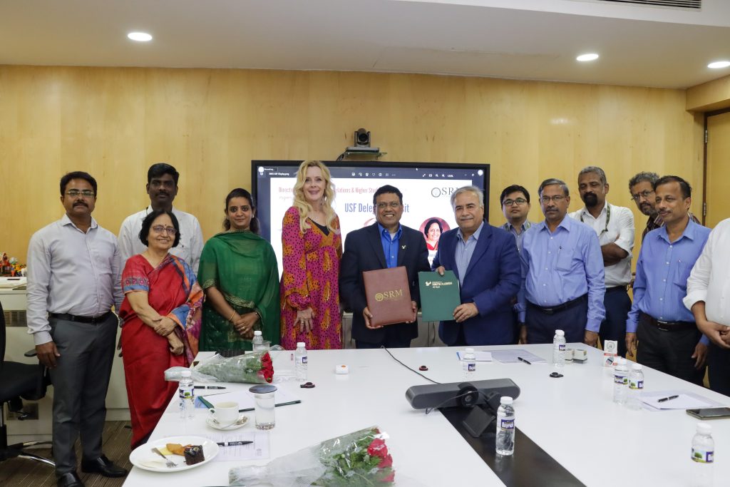


- Prof. Vandana Swami October 27, 2023
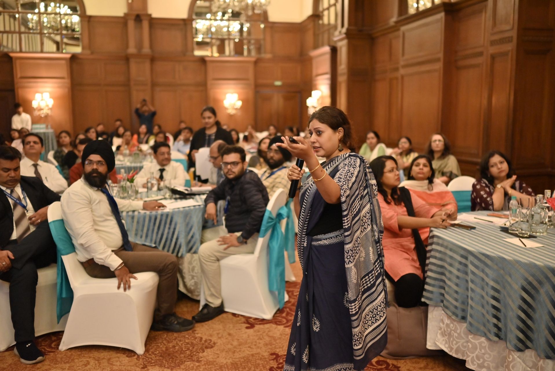
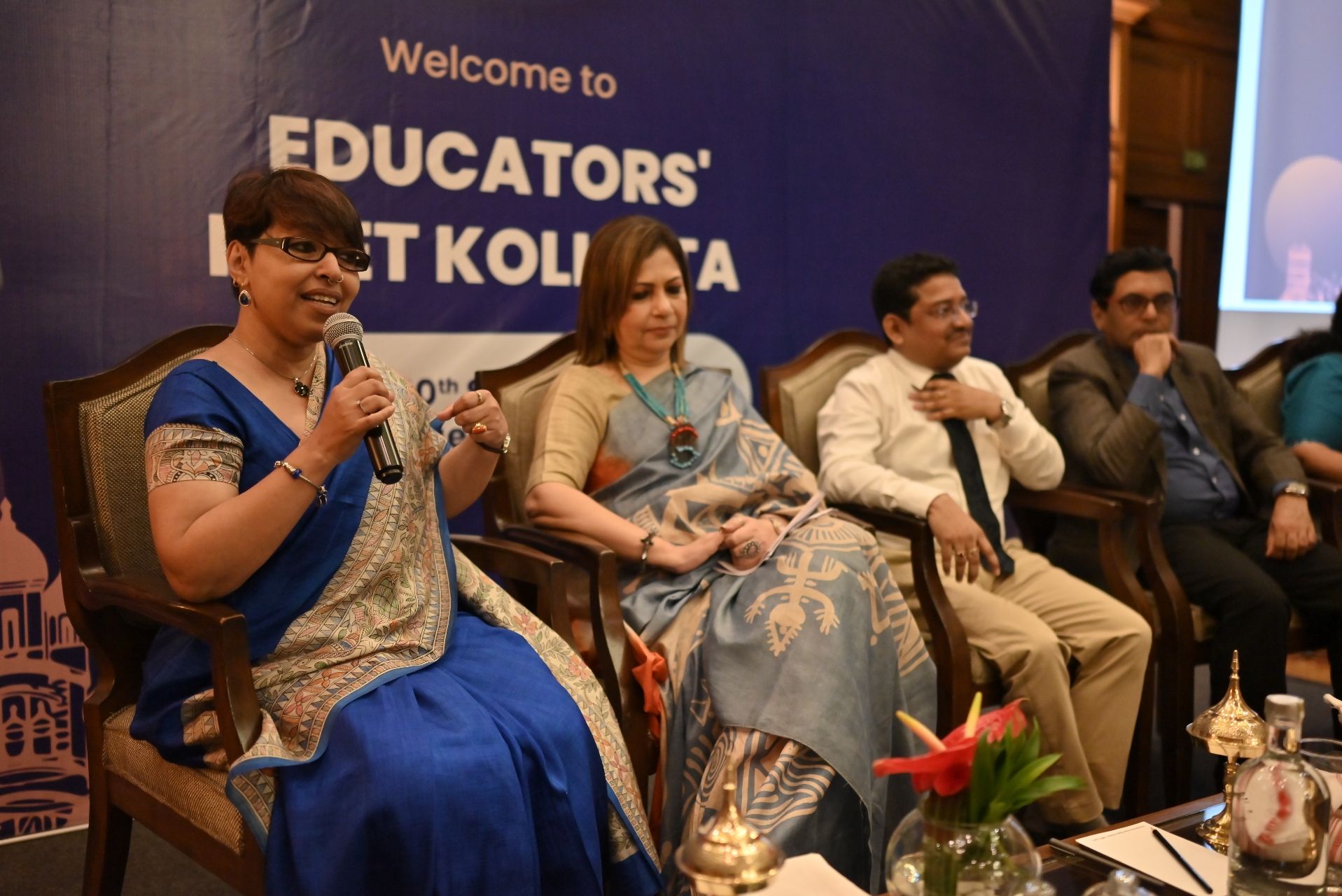
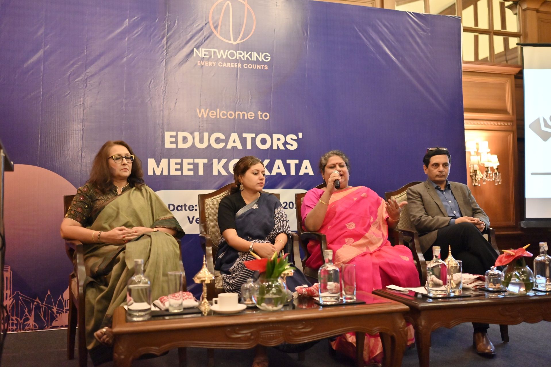
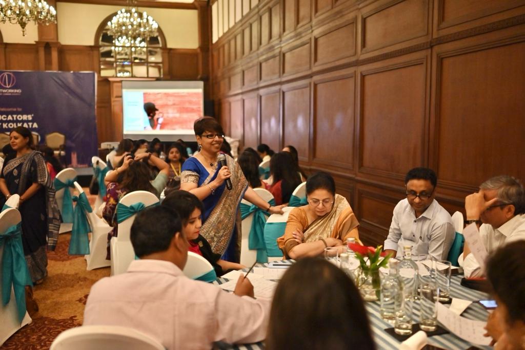
- Empowering the Future of Education: SRMAP at Educators’ Meet October 27, 2023
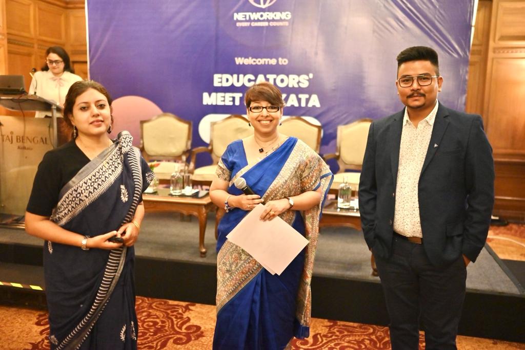
A transformative event in the field of education unfolded at the prestigious Taj Bengal Kolkata on September 30, 2023, as Networking, the event organiser, brought together visionaries, educators, and leaders from renowned institutions for a day of enlightening discussions. The symposium featured an engaging workshop on “Innovative Teaching Methods” and a panel discussion by acclaimed scholars from SRM University-AP and others on “Addressing Inclusivity in Education”.
SRM University-AP shared the stage with Mahindra University Hyderabad as presenters, sharing their insights into the dynamic world of academia. Their presentations provided a roadmap for educators to navigate the evolving landscape of teaching and learning. The event welcomed an illustrious audience, including the principals of some of Kolkata’s most esteemed schools, such as Don Bosco School, National English School, M P Birla Foundation Higher Secondary School, Ashok Hall Girls’ School, Sushila Birla Girls’ School, and Indus Valley World School and many more. This convergence of educational leaders was a testament to the growing need for innovation and inclusivity in the modern education system.
The workshop on Innovative Teaching Methods, led by SRM University-AP, aimed to empower educators with cutting-edge pedagogical tools and approaches. Presenters emphasised the need for adaptive learning, technology integration, and the nurturing of critical thinking skills. Attendees gained practical insights on how to create engaging, student-centered classrooms that inspire curiosity and creativity. The panel discussion on “Addressing Inclusivity in Education” was a powerful forum for introspection and collaboration. Renowned educator Dr Srabani Basu from SRM University-AP led the discourse on fostering an inclusive learning environment. The discussion revolved around strategies for accommodating diverse learning styles, ensuring equitable opportunities for all, and the role of education in shaping empathetic, well-rounded individuals.
A grand canvas was painted with discussions on “Preparing Students for Future Careers.” This event was more than just a meeting; it was a symphony of ideas, a platform for forging meaningful connections, and a springboard to a future of innovation and progress in education. The collaborative energy and innovative spirit that permeated the event offered a glimpse into the future of education. Participants left with a deeper understanding of the transformative power of innovative teaching methods and a collective commitment to make education accessible and inclusive for all. At SRM University-AP, we believe that events like these are pivotal in shaping the future of education. We are committed to embracing innovative teaching methods and fostering inclusivity to prepare our students for the dynamic and ever-evolving careers of the future.
Continue reading → - Dr Sapna Mishra October 27, 2023
- Dr Daigy Varghese October 27, 2023
- Best Paper Award: Accorded to Dr Supen Kumar at MRAE 2023 October 27, 2023
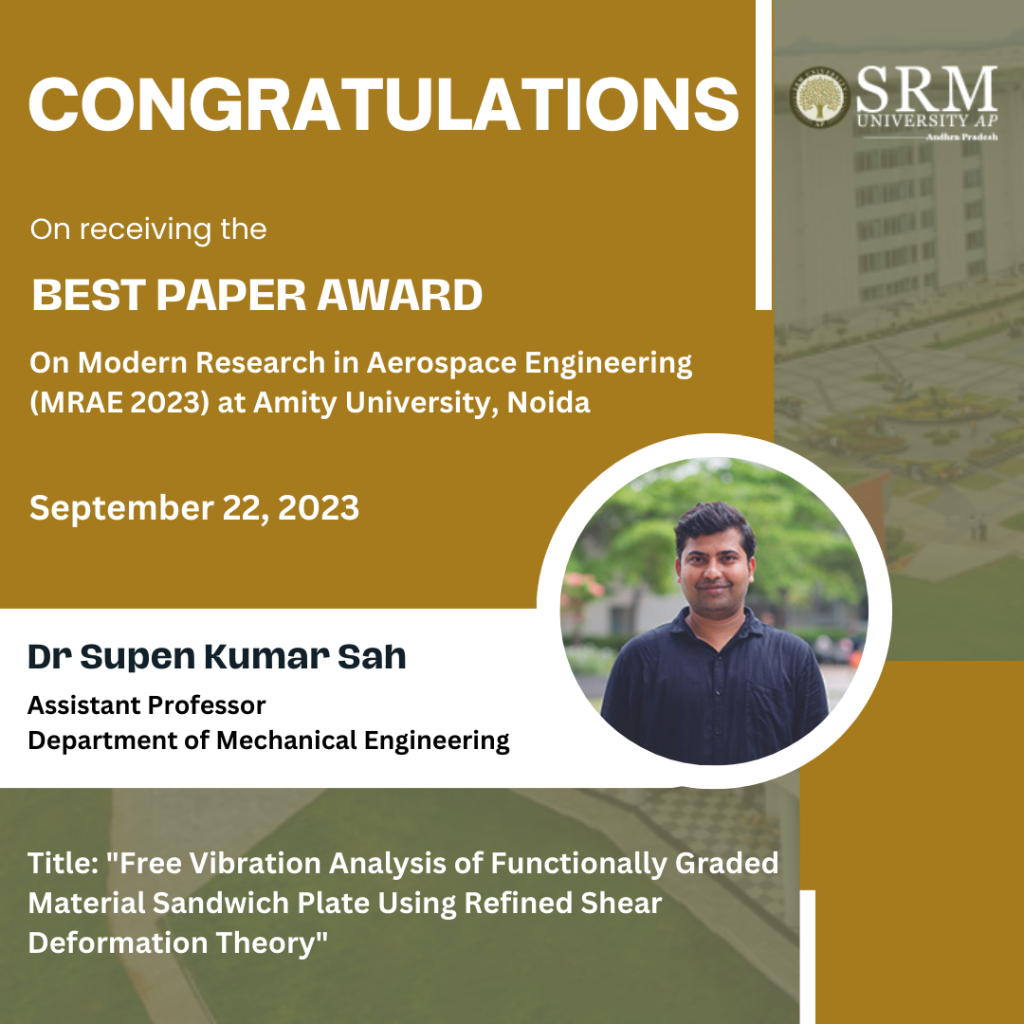
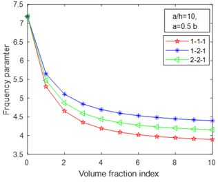
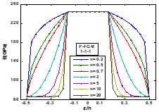
The Department of Mechanical Engineering is delighted to share that Dr Supen Kumar Sah, Assistant Professor, Department of Mechanical Engineering, has received the best paper award for his paper titled “Free Vibration Analysis of Functionally Graded Material Sandwich Plate Using Refined Shear Deformation Theory” in the 2nd International Conference on Modern Research in Aerospace Engineering (MRAE 2023). Dr Supen collaborated with Saloni Malviya of VIT, Bhopal, for the research paper. The paper explores the intricate dynamics of functionally graded material sandwich plates, employing a refined deformation theory. Dr Sah’s exceptional work has not only contributed to the scientific community but has also demonstrated his dedication and passion for advancing knowledge in the field of materials science and engineering.
Abstract
In the present study, free vibration analysis of a functionally graded material sandwich plate has been carried out using refined shear deformation theory. The shear correction factor is not needed since the parabolic variation of shear strain through the thickness is in such a way that shear stresses vanish on the plate surfaces. Hamilton’s principle is used for the derivation of the equation of motion for the theory. Additionally, Navier’s solution is used to obtain the eigenvalue equation for the sandwich plate. The three variants of sandwich plate are chosen for the analysis. To carry out the free vibration analysis three different types of FGM sandwich plate models namely 1-1-1, 1-2-1, and 2-2-1 have been considered. A power law defines the volume fraction index and the material properties of the individual layers of the sandwich plate. Lastly, the impact of parameters such as volume fraction, aspect ratio, and length-to-width ratio on frequency parameters is investigated.
Future Research Plans
• Modelling and Analysis of porous uni and multi-directional Functionally Graded Material (FGM) plates to obtain the impact of porosity distributions over structural responses.
• Analytical and finite Element Solutions for static and dynamic response of FGM sandwich plates employing non-polynomial shear deformation theories under elastic foundation.