
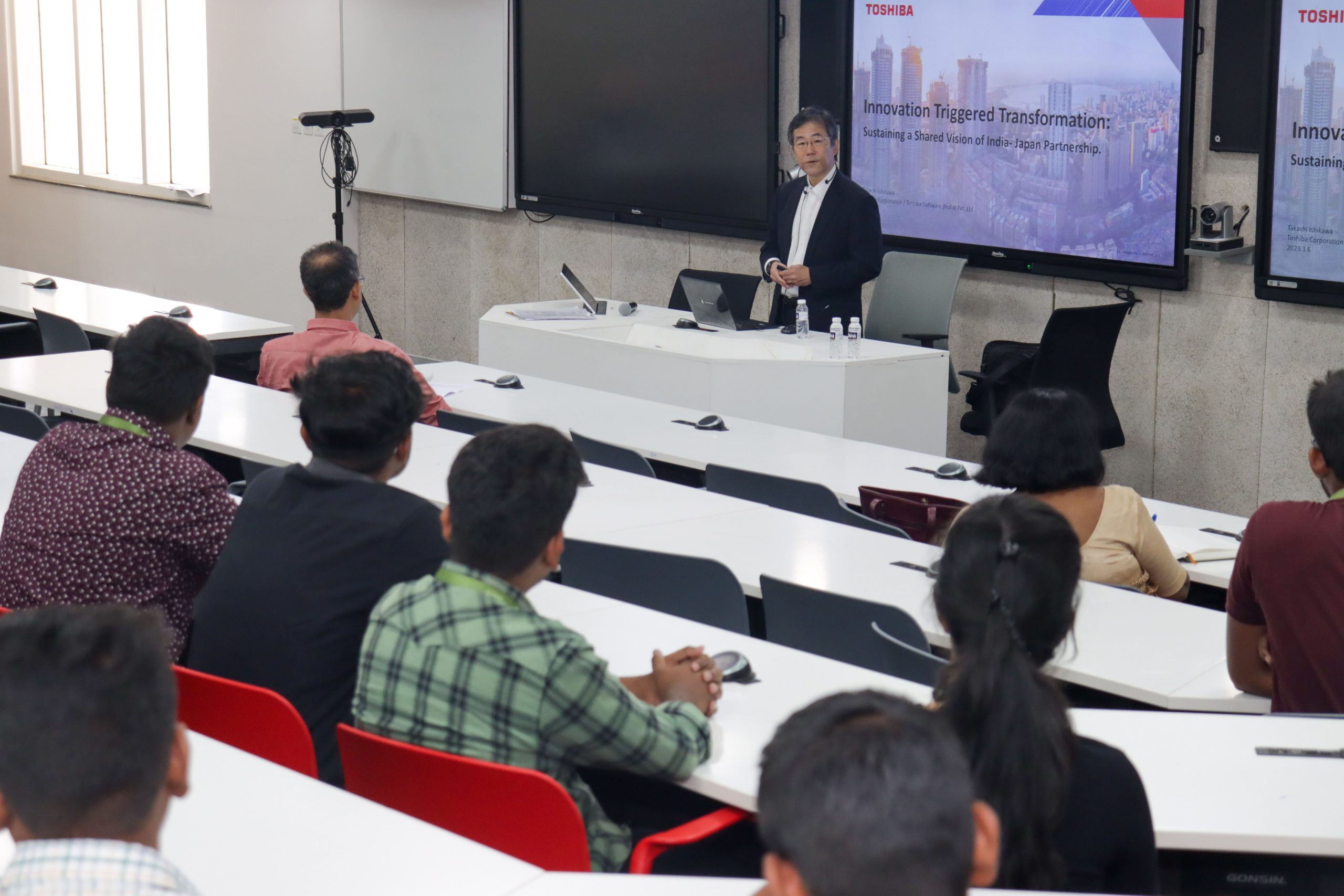
“Your Career in Business”- Insights from Mr Takashi Ishikawa
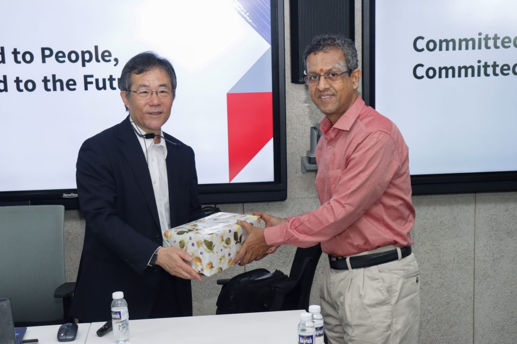
Visits from Big Techs offer an opportunity for young and potential students of management to develop future aspirations and shape their careers. The Paari School of Business organised a visit from the Tech Giant Mr Takashi Ishikawa, the Managing Director and Chairman of Toshiba Software India on March 06, 2023. The experienced business leader interacted with students and shared insight on prospective career opportunities and employment strategies for budding business managers. He encouraged students to explore different career paths and pursue their passions and interests. Mr Ishikawa emphasized the importance of continuous learning and development and encouraged students to pursue lifelong learning and stay current with the latest industry trends and technologies.
Mr Ishikawa also discussed the company’s recent developments and initiatives, including its focus on digital transformation and the development of innovative technologies. In addition to discussing the company’s initiatives. The visit has proved to be a beneficial opportunity for students to learn about the regional ecosystem of Toshiba Software and gain insights on career development from a seasoned industry leader. His emphasis on collaboration, innovation, and lifelong learning serves as a valuable reminder of the skills and qualities necessary for success in today’s dynamic business environment.

- Published in Departmental News, Management, News, Paari Current Happenings
Developing and Implementing Successful Marketing Strategies for Executives
“Intellectual growth should commence at birth and cease only at death- Albert Einstein”.
In today’s business world, technology is driving change, which in turn requires professionals to continuously upgrade their skills to stay efficient and relevant. Executive programmes, when well-designed, can be instrumental in this process by not only helping professionals acquire new skills, but also by facilitating the creation of a valuable peer network. The curriculum of executive programmes is specifically designed to impart knowledge and skills necessary for executives to excel amidst the challenges of the current business environment.
Focus of Executive Education Programmes?
The modern business world is in a constant state of evolution, with new dynamics emerging that require professionals to learn new skills and adapt to changing conditions. Some of these dynamics include:
Technological Advancement: Technological innovations are driving business growth and creating new opportunities at a rapid pace. Professionals who fail to keep up with these advancements risk becoming irrelevant.
Cut-throat Competition: The current business environment is characterised by intense competition, with new players entering the market and disrupting traditional business models.

Well-aware consumers: Modern consumers are well informed and have higher expectations from organisations. To remain competitive, businesses must adapt to changing consumer demands.
Agility and Adaptability: Due to the dynamic nature of the business environment, organisations are expected to be flexible and able to adapt to changing market conditions and consumer preferences. As a result, businesses expect their employees to be up-to-date, adaptable, and tech-savvy. In the light of this, executive education programmes focus on addressing the challenges posed by the emerging dynamics. Some of the focused areas are:
Leadership Development: To navigate the challenges of the modern business world, there is a growing need for confident and effective leaders. Executive programmes focus on developing leadership qualities among their students..
Digital Learning and Analytics: Data analytics has become increasingly important in business decision-making. Executive programmes provide training on software and tools that can help executives analyse and interpret data.
Entrepreneurship Skills: Innovative thinking and entrepreneurial skills are essential for driving business growth. As a result, executive programmes focus on developing these skills among their students.
Social Responsibility: Business organisations have a role to play in addressing social problems. Hence, executive programmes sensitise the students about the social issues and train them to contribute to social good.
EMBA- A Complete Package.
Executive MBA (EMBA) programmes are offered by numerous reputable institutions worldwide, with the goal of bridging the gap between executives’ current skillsets and the skills they need to excel in their careers. The EMBA curriculum is highly practical and emphasises the development of leadership qualities, data-driven decision-making, innovation, risk-taking, and more. Additionally, EMBA programmes offer courses in business ethics, which teach students to act responsibly in their business practices.
Individuals who enrol in an EMBA programme will engage in courses grounded in leadership and strategic theories. They will learn how to utilise critical thinking to make informed business decisions and establish relationships with peers to expand their professional networks. In summary, EMBA programmes provide an excellent opportunity for professionals to upgrade their skills, build strong networks, and advance in their careers.
- Published in Blog, Management
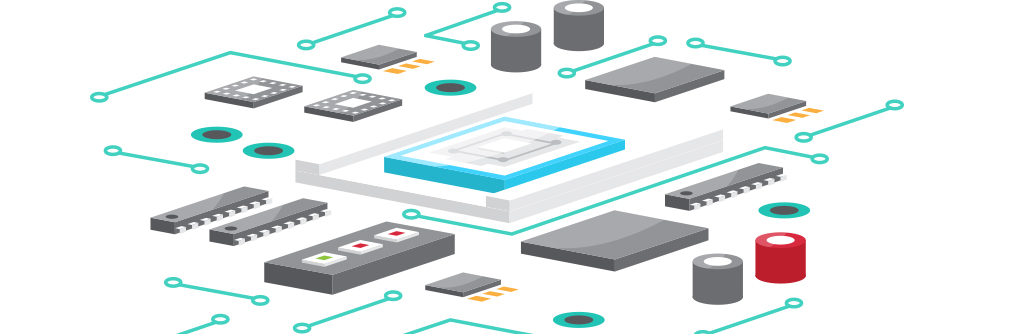
The Rise of Semiconductor Industry in India: Job Prospects for Engineers and Innovators
By Prof Y Siva Sankar
Professor of Practice, Department of Electronics and Communication Engineering
The time is right to hop onto the semiconductor bandwagon in India as the semiconductor industry in India is still in its early stages and poised for huge growth compared to some of the other major players in the global semiconductor market, such as the United States, South Korea, Japan, Taiwan, and China. The industry has been growing rapidly in recent years and is expected to play an increasingly important role in the global semiconductor ecosystem in the coming years.
According to a report by the India Electronics and Semiconductor Association (IESA), the Indian semiconductor industry was valued at approximately $36 billion in 2020. This includes the sales of integrated circuits (ICs), diodes, transistors, and other semiconductor products. The industry is expected to grow at a compound annual growth rate (CAGR) of around 22% between 2020 and 2025, reaching a value of $84 billion by 2025.
According to a report by Research and Markets, the global semiconductor market was valued at $464.1 billion in 2020 and is expected to reach $804.3 billion by 2026, growing at a CAGR of 9.3% between 2021 and 2026. The report highlights that the Asia-Pacific region, which includes India, is the largest market for semiconductors, accounting for over 50% of the global market share.
India’s semiconductor industry is expected to benefit from the global growth in demand for semiconductors, driven by the increasing adoption of technologies such as 5G, artificial intelligence, and the Internet of Things (IoT) in various industries. In addition, India is a major consumer of semiconductor products, but most of these products are imported. The Indian government has recognized the potential of the semiconductor industry and has taken several steps to promote its growth in the country.
Some of the key initiatives are:
- Make in India: The Make in India initiative, launched in 2014, aims to promote India as a global manufacturing hub by providing various incentives and reducing the regulatory burden on businesses. The initiative aims to increase the share of manufacturing in India’s GDP from 16% to 25% by 2025.
- National Policy on Electronics: The National Policy on Electronics (NPE) was launched in 2019 to promote the domestic manufacturing of electronic products and increase the value added in the electronics sector. The policy aims to create a conducive environment for the industry and attract foreign investment in the sector.
- Electronics Development Fund: The Electronics Development Fund (EDF) was set up in 2012 to financially support domestic companies involved in electronics design and manufacturing. The fund provides seed capital, venture capital, and debt financing to eligible companies.
- Modified Special Incentive Package Scheme: The Modified Special Incentive Package Scheme (M-SIPS) was launched in 2012 to provide capital subsidies to domestic companies to set up new electronics manufacturing units or expand existing ones. The scheme also includes reimbursement of central and state taxes and duties.
- Electronic Manufacturing Clusters: The government has set up Electronic Manufacturing Clusters (EMCs) across the country to provide world-class infrastructure and facilities to domestic and foreign companies for electronics manufacturing. The EMCs offer various incentives to eligible companies, such as tax exemptions, subsidies, and reimbursements.
Another significant step taken by the government is establishing a semiconductor wafer fab manufacturing facility in India. In 2020, the government announced the setting up of a Rs 6,900-crore ($941 million) semiconductor wafer fab manufacturing facility in Prayagraj, Uttar Pradesh. This facility is expected to boost the country’s semiconductor manufacturing capabilities and reduce its deep import dependence furthermore; several leading semiconductor companies have established their research and development (R&D) centres in India, taking advantage of the country’s vast talent pool and cost-effective workforce. These R&D centres are involved in developing cutting-edge semiconductor technologies and designing chips for various applications. These companies include Intel, Qualcomm, Samsung, Texas Instruments, and Broadcom.
- Published in Engineering
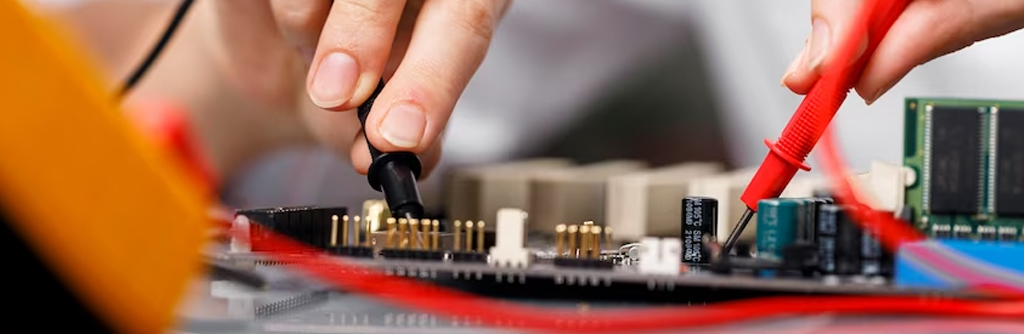
Opportunities and Career Paths in the Semiconductor Industry
According to a report by the India Semiconductor Association, the semiconductor industry in India is expected to create 1.75-2 million direct and indirect jobs by 2025. The report also stated that the industry had created 400,000 direct and indirect employment as of 2018.
The report highlighted that the demand for skilled professionals in the semiconductor industry is expected to increase across various job roles and functions, including research and development, design, manufacturing, testing, quality control, and sales and marketing.
In terms of salaries, the semiconductor industry in India offers competitive remuneration packages to skilled professionals. The average salary for a design engineer in the semiconductor industry in India is around INR 9-10 lakhs per annum, while the salary for a project manager can range from INR 15-25 lakhs per annum. Salaries for senior-level positions, such as director or vice president, can range from INR 50-100 lakhs per annum.

The semiconductor industry in India also offers good career growth opportunities, with skilled professionals able to progress to senior-level positions within a few years. The industry sector provides opportunities for professionals to work on cutting-edge technologies and contribute to developing innovative products.
The semiconductor industry is large and diverse, with many different job roles and career paths available. Some of the most common job roles in the semiconductor industry include the following:
1. Semiconductor Process Engineer:
A Semiconductor Process Engineer is responsible for designing and developing processes for manufacturing semiconductor devices such as integrated circuits, microprocessors, and memory chips. They work closely with other engineers and technicians to optimize production processes and ensure that the final products meet quality and performance standards.
The job role of a Semiconductor Process Engineer can vary depending on the specific industry and company they work for, but generally, their duties include:
- Developing and improving semiconductor manufacturing processes and equipment
- Conducting experiments and analyzing data to identify process improvements
- Designing and implementing process control systems to monitor and optimize production
- Troubleshooting and resolving process-related issues to minimize downtime and maintain production schedules
Some of the skills required for a Semiconductor Process Engineer include:
- Strong understanding of semiconductor manufacturing processes and equipment
- Proficiency in data analysis and statistical process control
- Familiarity with CAD tools, modeling software, and simulation techniques
- Experience in process development, optimization, and validation
Overall, a Semiconductor Process Engineer ensures the production processes are optimized for maximum efficiency and high-quality products.
- Published in Engineering
Semiconductor Design Engineer
2. Semiconductor Design Engineer
A Semiconductor Design Engineer is responsible for designing and developing semiconductor components and systems such as microprocessors, memory chips, and integrated circuits. They work closely with other engineers, including process engineers, to ensure their designs can be manufactured using existing or new production processes.
The job role of a Semiconductor Design Engineer can vary depending on the specific industry and company they work for, but generally, their duties include:
- Developing and implementing semiconductor design methodologies, processes, and standards
- Designing and testing semiconductor components and systems using CAD tools and simulation software
- Collaborating with cross-functional teams, including process engineers, testing engineers, and project managers, to ensure successful design and product development
- Conducting feasibility studies and analysing technical requirements to guide design decisions
- Ensuring that designs meet performance, power, and cost targets while adhering to quality and safety standards
- Preparing and reviewing design documentation, including schematics, layouts, and test plans
- Troubleshooting and resolving design-related issues to ensure successful product development and release
Some of the skills required for a Semiconductor Design Engineer include:
- Strong understanding of semiconductor design methodologies, processes, and standards
- Proficiency in CAD tools and simulation software for designing semiconductor components and systems
- Familiarity with semiconductor manufacturing processes and their impact on design
- Experience in designing and testing complex semiconductor systems
Overall, a Semiconductor Design Engineer ensures that semiconductor components and systems are designed to meet performance, cost, and quality targets while adhering to safety and regulatory standards.
- Published in Engineering
Semiconductor Test Engineer
3. Semiconductor Test Engineer
A Semiconductor Test Engineer is responsible for designing and developing testing processes and systems for semiconductor devices such as microprocessors, memory chips, and integrated circuits. They work closely with other engineers, including design and process engineers, to ensure the testing processes are optimized for the specific device.
The job role of a Semiconductor Test Engineer can vary depending on the specific industry and company they work for, but generally, their duties include:
- Developing and implementing test methodologies, processes, and standards for semiconductor devices
- Designing and developing test hardware and software for semiconductor testing systems
- Collaborating with cross-functional teams, including design, process, and packaging engineers, to ensure successful product testing
- Conducting feasibility studies and analysing technical requirements to guide testing process development
- Ensuring that testing processes meet performance, power, and cost targets while adhering to quality and safety standards
- Preparing and reviewing test documentation, including test plans and test reports
- Troubleshooting and resolving test-related issues to ensure successful product testing and release
Some of the skills required for a Semiconductor Test Engineer include:
- Strong understanding of semiconductor testing methodologies, processes, and standards
- Proficiency in testing hardware and software for semiconductor devices
- Familiarity with semiconductor manufacturing processes and their impact on testing
- Experience in designing and developing testing processes and systems for semiconductor devices
Overall, a Semiconductor Test Engineer ensures that semiconductor devices are tested and validated to meet performance, cost, and quality targets while adhering to safety and regulatory standards.
- Published in Engineering
Design for Testability (DFT) Engineer

4. Design for Testability (DFT) Engineer
A DFT (Design for Testability) Engineer is responsible for designing and implementing testability features in semiconductor devices such as microprocessors, memory chips, and integrated circuits. They work closely with other engineers, including design, test, and manufacturing engineers, to ensure the device can be efficiently tested during manufacturing.
The job role of a DFT Engineer can vary depending on the specific industry and company they work for, but generally, their duties include:
- Developing and implementing testability features in semiconductor device designs
- Collaborating with design and test engineers to ensure that the device can be efficiently tested during the manufacturing process
- Analysing and optimising design for testability, including scan chain insertion and boundary scan implementation
- Creating and reviewing test plans and test coverage reports
- Designing and implementing functional test vectors and test programs for the device
- Developing and implementing fault models for the device to improve test coverage
- Troubleshooting and resolving DFT-related issues to ensure successful manufacturing and product release
Some of the skills required for a DFT Engineer include:
- Strong understanding of DFT methodologies, processes, and standards
- Proficiency in DFT tools and software for semiconductor devices
- Familiarity with semiconductor manufacturing processes and their impact on DFT
- Experience in designing and implementing DFT features in semiconductor device designs
Overall, a DFT Engineer ensures that semiconductors are designed with the necessary testability features to improve manufacturing efficiency and product quality while adhering to safety and regulatory standards.
- Published in Engineering