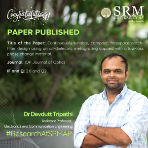
 This research paper titled, “Continuously-tunable, compact, freespace notch-filter design using an all-dielectric metagrating capped with a low-loss phase change material” by Dr Devdutt Tripathi, Assistant Professor, Department Electronics and Communication Engineering explores the use of active metasurfaces combined with phase change materials (PCMs) to enhance optical technologies thereby enhancing optical technologies across various sectors including telecommunications and imaging sectors.
Abstract:
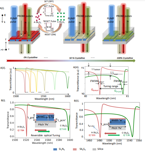
Active metasurfaces utilising phase change materials (PCMs) are currently under investigation for applications in free-space optical communication, optical signal processing, neuromorphic photonics, quantum photonics, and compact LiDAR. Attention has now turned towards novel PCM like Sb2S3 which exhibit lower optical absorption and reasonable values of refractive-index contrast in comparison to traditional data-storage PCM. We propose and numerically study the class of all-dielectric metagratings capped with low-loss PCM and predict the possibility of continuously tunable resonances whose quality factors degrade gracefully during the amorphous-to-crystalline phase transition of the PCM. Specifically, we consider the CMOS-compatible silicon-nitride on silica substrate material platform for simple and asymmetric metagratings (in particular, the symmetric-broken dimerization) and Sb2S3 capping. Our numerical study predicts that notch-filters operating around the 1550 nm NIR wavelength window can be achieved with tuning range of over 76 nm with Q-factors ranging from 784 (amorphous-phase) to 510 (crystalline-phase) (a degradation in Q of about 35%) and insertion loss of about 0.9 dB. These performance figures are a significant improvement over previously published designs utilizing data-storage PCMs and other traditional notch-filter mechanisms. We examine the influence of grating dimerization and geometrical parameters on performance metrics of the notch-filter and predict the possibility to trade-off rejection-band and in-band spectral transmission properties. Lastly, we perform a study of an all-optical phase change mechanism. Our study is promising for the miniaturization of tunable notch-filter based optical systems.
Explanation in Layperson’s Terms:
This research explores the use of advanced materials called metasurfaces (engineered materials especially in a 2D thin film structure), combined with phase change materials (PCMs- Semiconducting alloys of the Chalcogen family), for improving already existing and emergent technologies such as Optical communication, LiDAR (an acronym for Light Detection and Ranging), and Quantum photonics. Metasurfaces are thin layers with typical thickness ranging from a few hundred nanometers to several micrometers that can manipulate light in unique ways. In this study, the focus is on a specific PCM, Antimony Trisulphide (Sb2S3), which exhibits lower light absorption and better control over how it interacts with the incident light compared to traditional PCMs such as GST225 (Germanium Antimony Telluride) used in data storage. We propose a new design of metasurfaces, called metagratings, that can be “tuned” by changing the state of the PCM between amorphous and crystalline forms. The study predicts that these metasurfaces can be used to create notch filters, which block specific wavelengths of light, particularly around the 1550 nm range commonly used in fiber optics. When the PCM switches states, the filter can shift by 76 nm, with only a minor decrease in performance, about 35%. The study also looks at how small changes in the shape and structure of the metagratings can fine-tune their performance, allowing for a balance between filtering strength and light transmission. Overall, this research points to a promising way of miniaturizing and improving tunable optical filters for a range of high-tech applications.
Practical Implications:
This research has several practical implications:
1. Optical Communication: It can improve free-space optical
communication by offering tunable filters to enhance signal clarity and reduce interference.
2. Miniaturized LiDAR: Smaller, more efficient LiDAR systems for autonomous vehicles and 3D mapping can be developed.
3. Optical Signal Processing: Faster, more efficient photonic circuits could be created for data processing and telecommunications.
4. Neuromorphic and Quantum Photonics: The tunable metasurfaces can support advanced computing and quantum technologies by precisely controlling light.
5. Energy Efficiency: Sb₂S₃ uses less power than traditional materials, making devices more energy-efficient.
6. Sensing and Imaging: It can improve sensors and imaging systems by allowing more precise wavelength control.
7. CMOS Compatibility: The research can be integrated into existing semiconductor technologies, facilitating mass production.
Collaborators:
1. Prof. Hardik S. Vyas: Assistant Professor in Department of ICT, PDEU, Gandhinagar, Gujarat.
2. Prof. Ravi S Hegde, Associate Professor in Department of Electrical Engineering, IIT Gandhinagar, Gujarat.
Future Research Plans:
Research in Metasurface can be explored towards various applications such as imaging, microscopy as well as communication.
Article Link:https://iopscience.iop.org/article/10.1088/2040-8986/ad80a6


