
All Management News
- Physical Design (PD) Engineer March 24, 2023

5. Physical Design (PD) Engineer
A Physical Design Engineer is responsible for designing and implementing the physical layout of semiconductor devices such as microprocessors, memory chips, and integrated circuits. They work closely with other engineers, including design, verification, and manufacturing engineers, to ensure that the device is optimised for performance, power, and manufacturability.
The job role of a Physical Design Engineer can vary depending on the specific industry and company they work for, but generally, their duties include:
- Designing and implementing the physical layout of semiconductor devices using tools such as Cadence, Synopsys, and Mentor Graphics
- Collaborating with design, verification, and manufacturing engineers to optimise the device for performance, power, and manufacturability
- Analysing and optimising the device for timing, power, noise, and thermal characteristics
- Creating and reviewing design rules and design constraints
- Developing and implementing design methodologies and flow to improve design efficiency and quality
- Preparing and reviewing design documentation, including floor plans, power grid, and package designs
- Troubleshooting and resolving physical design-related issues to ensure successful manufacturing and product release.
Some of the skills required for a Physical Design Engineer include:
- Strong understanding of physical design methodologies, processes, and standards
- Proficiency in physical design tools and software such as Cadence, Synopsys, and Mentor Graphics
- Familiarity with semiconductor manufacturing processes and their impact on physical design
- Experience in designing and implementing physical layouts of semiconductor devices
Overall, a Physical Design Engineer ensures that semiconductor devices are optimised for performance, power, and manufacturability while adhering to safety and regulatory standards.
Continue reading → - Design for Testability (DFT) Engineer March 24, 2023

4. Design for Testability (DFT) Engineer
A DFT (Design for Testability) Engineer is responsible for designing and implementing testability features in semiconductor devices such as microprocessors, memory chips, and integrated circuits. They work closely with other engineers, including design, test, and manufacturing engineers, to ensure the device can be efficiently tested during manufacturing.
The job role of a DFT Engineer can vary depending on the specific industry and company they work for, but generally, their duties include:
- Developing and implementing testability features in semiconductor device designs
- Collaborating with design and test engineers to ensure that the device can be efficiently tested during the manufacturing process
- Analysing and optimising design for testability, including scan chain insertion and boundary scan implementation
- Creating and reviewing test plans and test coverage reports
- Designing and implementing functional test vectors and test programs for the device
- Developing and implementing fault models for the device to improve test coverage
- Troubleshooting and resolving DFT-related issues to ensure successful manufacturing and product release
Some of the skills required for a DFT Engineer include:
- Strong understanding of DFT methodologies, processes, and standards
- Proficiency in DFT tools and software for semiconductor devices
- Familiarity with semiconductor manufacturing processes and their impact on DFT
- Experience in designing and implementing DFT features in semiconductor device designs
Overall, a DFT Engineer ensures that semiconductors are designed with the necessary testability features to improve manufacturing efficiency and product quality while adhering to safety and regulatory standards.
Continue reading → - Semiconductor Test Engineer March 24, 2023
3. Semiconductor Test Engineer

A Semiconductor Test Engineer is responsible for designing and developing testing processes and systems for semiconductor devices such as microprocessors, memory chips, and integrated circuits. They work closely with other engineers, including design and process engineers, to ensure the testing processes are optimized for the specific device.
The job role of a Semiconductor Test Engineer can vary depending on the specific industry and company they work for, but generally, their duties include:
- Developing and implementing test methodologies, processes, and standards for semiconductor devices
- Designing and developing test hardware and software for semiconductor testing systems
- Collaborating with cross-functional teams, including design, process, and packaging engineers, to ensure successful product testing
- Conducting feasibility studies and analysing technical requirements to guide testing process development
- Ensuring that testing processes meet performance, power, and cost targets while adhering to quality and safety standards
- Preparing and reviewing test documentation, including test plans and test reports
- Troubleshooting and resolving test-related issues to ensure successful product testing and release
Some of the skills required for a Semiconductor Test Engineer include:
- Strong understanding of semiconductor testing methodologies, processes, and standards
- Proficiency in testing hardware and software for semiconductor devices
- Familiarity with semiconductor manufacturing processes and their impact on testing
- Experience in designing and developing testing processes and systems for semiconductor devices
Overall, a Semiconductor Test Engineer ensures that semiconductor devices are tested and validated to meet performance, cost, and quality targets while adhering to safety and regulatory standards.
Continue reading → - Semiconductor Design Engineer March 23, 2023

2. Semiconductor Design Engineer
A Semiconductor Design Engineer is responsible for designing and developing semiconductor components and systems such as microprocessors, memory chips, and integrated circuits. They work closely with other engineers, including process engineers, to ensure their designs can be manufactured using existing or new production processes.
The job role of a Semiconductor Design Engineer can vary depending on the specific industry and company they work for, but generally, their duties include:
- Developing and implementing semiconductor design methodologies, processes, and standards
- Designing and testing semiconductor components and systems using CAD tools and simulation software
- Collaborating with cross-functional teams, including process engineers, testing engineers, and project managers, to ensure successful design and product development
- Conducting feasibility studies and analysing technical requirements to guide design decisions
- Ensuring that designs meet performance, power, and cost targets while adhering to quality and safety standards
- Preparing and reviewing design documentation, including schematics, layouts, and test plans
- Troubleshooting and resolving design-related issues to ensure successful product development and release
Some of the skills required for a Semiconductor Design Engineer include:
- Strong understanding of semiconductor design methodologies, processes, and standards
- Proficiency in CAD tools and simulation software for designing semiconductor components and systems
- Familiarity with semiconductor manufacturing processes and their impact on design
- Experience in designing and testing complex semiconductor systems
Overall, a Semiconductor Design Engineer ensures that semiconductor components and systems are designed to meet performance, cost, and quality targets while adhering to safety and regulatory standards.
Continue reading → - Opportunities and Career Paths in the Semiconductor Industry March 23, 2023
According to a report by the India Semiconductor Association, the semiconductor industry in India is expected to create 1.75-2 million direct and indirect jobs by 2025. The report also stated that the industry had created 400,000 direct and indirect employment as of 2018.
The report highlighted that the demand for skilled professionals in the semiconductor industry is expected to increase across various job roles and functions, including research and development, design, manufacturing, testing, quality control, and sales and marketing.
In terms of salaries, the semiconductor industry in India offers competitive remuneration packages to skilled professionals. The average salary for a design engineer in the semiconductor industry in India is around INR 9-10 lakhs per annum, while the salary for a project manager can range from INR 15-25 lakhs per annum. Salaries for senior-level positions, such as director or vice president, can range from INR 50-100 lakhs per annum.

The semiconductor industry in India also offers good career growth opportunities, with skilled professionals able to progress to senior-level positions within a few years. The industry sector provides opportunities for professionals to work on cutting-edge technologies and contribute to developing innovative products.
The semiconductor industry is large and diverse, with many different job roles and career paths available. Some of the most common job roles in the semiconductor industry include the following:
1. Semiconductor Process Engineer:
A Semiconductor Process Engineer is responsible for designing and developing processes for manufacturing semiconductor devices such as integrated circuits, microprocessors, and memory chips. They work closely with other engineers and technicians to optimize production processes and ensure that the final products meet quality and performance standards.
The job role of a Semiconductor Process Engineer can vary depending on the specific industry and company they work for, but generally, their duties include:
- Developing and improving semiconductor manufacturing processes and equipment
- Conducting experiments and analyzing data to identify process improvements
- Designing and implementing process control systems to monitor and optimize production
- Troubleshooting and resolving process-related issues to minimize downtime and maintain production schedules
Some of the skills required for a Semiconductor Process Engineer include:
- Strong understanding of semiconductor manufacturing processes and equipment
- Proficiency in data analysis and statistical process control
- Familiarity with CAD tools, modeling software, and simulation techniques
- Experience in process development, optimization, and validation
Overall, a Semiconductor Process Engineer ensures the production processes are optimized for maximum efficiency and high-quality products.
Continue reading → - The Rise of Semiconductor Industry in India: Job Prospects for Engineers and Innovators March 23, 2023
By Prof Y Siva Sankar
Professor of Practice, Department of Electronics and Communication EngineeringThe time is right to hop onto the semiconductor bandwagon in India as the semiconductor industry in India is still in its early stages and poised for huge growth compared to some of the other major players in the global semiconductor market, such as the United States, South Korea, Japan, Taiwan, and China. The industry has been growing rapidly in recent years and is expected to play an increasingly important role in the global semiconductor ecosystem in the coming years.
According to a report by the India Electronics and Semiconductor Association (IESA), the Indian semiconductor industry was valued at approximately $36 billion in 2020. This includes the sales of integrated circuits (ICs), diodes, transistors, and other semiconductor products. The industry is expected to grow at a compound annual growth rate (CAGR) of around 22% between 2020 and 2025, reaching a value of $84 billion by 2025.
According to a report by Research and Markets, the global semiconductor market was valued at $464.1 billion in 2020 and is expected to reach $804.3 billion by 2026, growing at a CAGR of 9.3% between 2021 and 2026. The report highlights that the Asia-Pacific region, which includes India, is the largest market for semiconductors, accounting for over 50% of the global market share.

India’s semiconductor industry is expected to benefit from the global growth in demand for semiconductors, driven by the increasing adoption of technologies such as 5G, artificial intelligence, and the Internet of Things (IoT) in various industries. In addition, India is a major consumer of semiconductor products, but most of these products are imported. The Indian government has recognized the potential of the semiconductor industry and has taken several steps to promote its growth in the country.
Some of the key initiatives are:
- Make in India: The Make in India initiative, launched in 2014, aims to promote India as a global manufacturing hub by providing various incentives and reducing the regulatory burden on businesses. The initiative aims to increase the share of manufacturing in India’s GDP from 16% to 25% by 2025.
- National Policy on Electronics: The National Policy on Electronics (NPE) was launched in 2019 to promote the domestic manufacturing of electronic products and increase the value added in the electronics sector. The policy aims to create a conducive environment for the industry and attract foreign investment in the sector.
- Electronics Development Fund: The Electronics Development Fund (EDF) was set up in 2012 to financially support domestic companies involved in electronics design and manufacturing. The fund provides seed capital, venture capital, and debt financing to eligible companies.
- Modified Special Incentive Package Scheme: The Modified Special Incentive Package Scheme (M-SIPS) was launched in 2012 to provide capital subsidies to domestic companies to set up new electronics manufacturing units or expand existing ones. The scheme also includes reimbursement of central and state taxes and duties.
- Electronic Manufacturing Clusters: The government has set up Electronic Manufacturing Clusters (EMCs) across the country to provide world-class infrastructure and facilities to domestic and foreign companies for electronics manufacturing. The EMCs offer various incentives to eligible companies, such as tax exemptions, subsidies, and reimbursements.
Another significant step taken by the government is establishing a semiconductor wafer fab manufacturing facility in India. In 2020, the government announced the setting up of a Rs 6,900-crore ($941 million) semiconductor wafer fab manufacturing facility in Prayagraj, Uttar Pradesh. This facility is expected to boost the country’s semiconductor manufacturing capabilities and reduce its deep import dependence furthermore; several leading semiconductor companies have established their research and development (R&D) centres in India, taking advantage of the country’s vast talent pool and cost-effective workforce. These R&D centres are involved in developing cutting-edge semiconductor technologies and designing chips for various applications. These companies include Intel, Qualcomm, Samsung, Texas Instruments, and Broadcom.
Continue reading → - IMUN Appreciation for Students at International Conference in Vietnam March 23, 2023
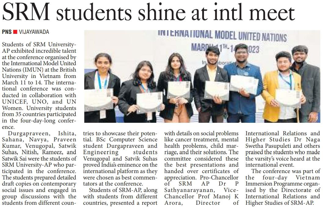
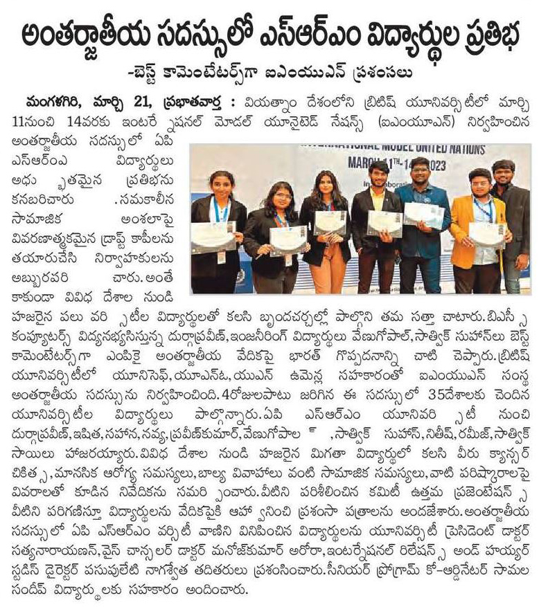
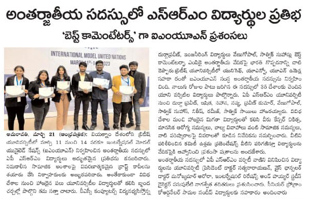
 Students of SRM University-AP exhibited incredible talent at the conference organised by the International Model United Nations (IMUN) at the British University in Vietnam from March 11 to 14, 2023. The international conference has been conducted in collaboration with UNICEF, UNO, and UN Women. University students from 35 countries participated in the four-day long conference.
Durgapraveen, Eeshitha, Sahana, Navya, Praveen Kumar, Venugopal, Satwik Suhas, Nitish, Rameez and Satwik Sai were the students of SRM University-AP who participated in the conference. Students prepared detailed draft copies on contemporary social issues and engaged in group discussions with students from different countries to showcase their potential. Along with students from other countries, they presented a report with details on social problems like cancer treatment, mental health problems, and child marriage and their solutions. The committee considered these the best presentations and handed over certificates of appreciation. Pro-Chancellor, Dr P Sathyanarayanan; Vice Chancellor, Prof. Manoj K Arora; Director of International Relations and Higher Studies, Dr Naga Swetha Pasupuleti; and others praised the students who made the varsity’s voice heard at the international conference.
The conference was part of the 4-day Vietnam Immersion Programme organised by the Directorate of International Relations and Higher Studies of SRM AP. The programme featured 10 students from the university. Diplomatic Talk from the embassies on recent global issues, MUN 101 and Training Sessions for the participants, Paper presentations on UNDP, WHO, UNSC, UNICEF, UNWoman & UNESCO, Social Night, cultural exchange, and networking with global participants, and Educational City Tour to explore the capital city, Hanoi were the highlights of the immersion programme.
Continue reading →


- Developing and Implementing Successful Marketing Strategies for Executives March 23, 2023
“Intellectual growth should commence at birth and cease only at death- Albert Einstein”.
In today’s business world, technology is driving change, which in turn requires professionals to continuously upgrade their skills to stay efficient and relevant. Executive programmes, when well-designed, can be instrumental in this process by not only helping professionals acquire new skills, but also by facilitating the creation of a valuable peer network. The curriculum of executive programmes is specifically designed to impart knowledge and skills necessary for executives to excel amidst the challenges of the current business environment.
Focus of Executive Education Programmes?
The modern business world is in a constant state of evolution, with new dynamics emerging that require professionals to learn new skills and adapt to changing conditions. Some of these dynamics include:
Technological Advancement: Technological innovations are driving business growth and creating new opportunities at a rapid pace. Professionals who fail to keep up with these advancements risk becoming irrelevant.
Cut-throat Competition: The current business environment is characterised by intense competition, with new players entering the market and disrupting traditional business models.

Well-aware consumers: Modern consumers are well informed and have higher expectations from organisations. To remain competitive, businesses must adapt to changing consumer demands.
Agility and Adaptability: Due to the dynamic nature of the business environment, organisations are expected to be flexible and able to adapt to changing market conditions and consumer preferences. As a result, businesses expect their employees to be up-to-date, adaptable, and tech-savvy. In the light of this, executive education programmes focus on addressing the challenges posed by the emerging dynamics. Some of the focused areas are:
Leadership Development: To navigate the challenges of the modern business world, there is a growing need for confident and effective leaders. Executive programmes focus on developing leadership qualities among their students..
Digital Learning and Analytics: Data analytics has become increasingly important in business decision-making. Executive programmes provide training on software and tools that can help executives analyse and interpret data.
Entrepreneurship Skills: Innovative thinking and entrepreneurial skills are essential for driving business growth. As a result, executive programmes focus on developing these skills among their students.
Social Responsibility: Business organisations have a role to play in addressing social problems. Hence, executive programmes sensitise the students about the social issues and train them to contribute to social good.
EMBA- A Complete Package.
Executive MBA (EMBA) programmes are offered by numerous reputable institutions worldwide, with the goal of bridging the gap between executives’ current skillsets and the skills they need to excel in their careers. The EMBA curriculum is highly practical and emphasises the development of leadership qualities, data-driven decision-making, innovation, risk-taking, and more. Additionally, EMBA programmes offer courses in business ethics, which teach students to act responsibly in their business practices.
Continue reading →
Individuals who enrol in an EMBA programme will engage in courses grounded in leadership and strategic theories. They will learn how to utilise critical thinking to make informed business decisions and establish relationships with peers to expand their professional networks. In summary, EMBA programmes provide an excellent opportunity for professionals to upgrade their skills, build strong networks, and advance in their careers. - International Conference at the British University in Vietnam: Students of SRM University Get IMUN Appreciation for Being the ‘Best Commentators’ March 23, 2023
Deccan Chronicle
Continue reading →

The Hindu

The Pioneer
News India Express

The Hans India

Eenadu

Visalandhra

Vartha
Surya

Andhra Patrika
- Maximising Electrochemical NH3 Production March 21, 2023

Significant measures have been undertaken to synthesise ammonia proficiently, the future renewable energy fuel for its wide range of applications in various sectors. On this account, a research paper titled “Oxygen functionalization-induced charging effect on boron active sites for high-yield electrochemical NH3 production” has been published by Prof. Ranjit Thapa, Professor, Department of Physics and his research scholar Mr Samadhan Kapse in the journal Nano-Micro Letters having an impact factor of 23.655.
Abstract
Ammonia has been recognized as the future renewable energy fuel because of its wide-ranging applications in H2 storage and transportation sector. In order to avoid the environmentally hazardous Haber–Bosch process, recently, the third-generation ambient ammonia synthesis has drawn phenomenal attention and thus tremendous efforts are devoted to developing efficient electrocatalysts that would circumvent the bottlenecks of the electrochemical nitrogen reduction reaction (NRR) like competitive hydrogen evolution reaction, poor selectivity of N2 on the catalyst surface. Herein, we report the synthesis of an oxygen-functionalised boron carbonitride matrix via a two-step pyrolysis technique. The conductive BNCO(1000) architecture, the compatibility of B-2pz orbital with the N-2pz orbital and the charging effect over B due to the C and O edge-atoms in a pentagon altogether facilitate N2 adsorption on the B edge-active sites. The optimum electrolyte acidity with 0.1 M HCl and the lowered anion crowding effect aid the protonation steps of NRR via an associative alternating pathway, which gives a sufficiently high yield of ammonia (211.5 μgh−1 mgcat−1) on the optimized BNCO(1000) catalyst with a Faradaic efficiency of 34.7% at −0.1 V vs RHE. This work thus offers a cost-effective electrode material and provides the contemporary idea about reinforcing the charging effect over the secured active sites for NRR by selectively choosing the electrolyte anions and functionalizing the active edges of the BNCO(1000) catalyst.

A brief summary of the research in layman’s terms
In summary, this work displayed the significant role of O and C doping within BN architecture to promote NRR on the edge B sites via an associative alternating mechanism. The gradual formation of the ideal structure was systematically studied by means of XPS and the electronic properties was investigated from NEXAFS. A greater impact was found on the charging effect of B centres due to O-functionalized edges that induced a greater charge density from B to the adsorbed N2, overcoming the potential determining steps for NRR. This work simultaneously highlighted the importance of the choice of electrolyte, where in 0.1 M HCl our catalyst BNCO(1000) yielded 211.5 μg h−1mgcat−1 of ammonia at −0.1 V vs RHE with a FE of 34.7%. It was experimentally found and theoretically supported that the bulky anions in H2SO4 and H3PO4 blocked the B active sites by a Lewis acid-base interaction between the B sites and the O ends of the anions, hence not suitable for this class of materials. Thus, the present work offered an overall idea of catalyst designing and the medium to retain a high and consistent NRR performance.
Social implications of the research
Nitrogen reduction reaction (NRR) performed electrochemically is regarded as a green and legitimate approach to ammonia synthesis and it has been intrinsically brought into the limelight by the worldwide research community, not only because of the immense use of ammonia in the agriculture and transportation sector but also due to urge to resolve the fallacies associated with the process. Primarily, the eternal problem persisting with NRR is the predominance of the combative hydrogen evolution reaction (HER) at the same potential range, which overpowers NRR over most of the catalyst surfaces, resulting in poor yield and Faradaic efficiency (FE) of ammonia production. Researchers thus majorly focus on varied catalyst development, which includes several strategies: (a) Selectivity of elements that would prefer binding with N2 over protons, (b) Blocking the HER active sites, (c) Phase-selective material designing, inhibiting HER at the active surface, (d) interface-engineering that would deviate the HER pathway inducing better Faradaic efficiency for NRR. Although either 1st-row transition metals or semimetals are regarded as more suitable candidates for NRR, a metal-free approach is rather preferred for the cost-effectiveness and simplicity of the process. Boron (B)-based electrocatalyst in this respect can act as a strong contender. The research also posits that Density functional theory is useful for the molecular level understanding to unveil the performance of different catalytic reactions.

Collaborations
- Ms Ashmita Biswas, Institute of Nano Science and Technology (INST), Sector-81, Mohali, Punjab 140306, India
- Mr Ramendra Sundar Dey, Institute of Nano Science and Technology (INST), Sector-81, Mohali, Punjab 140306, India