
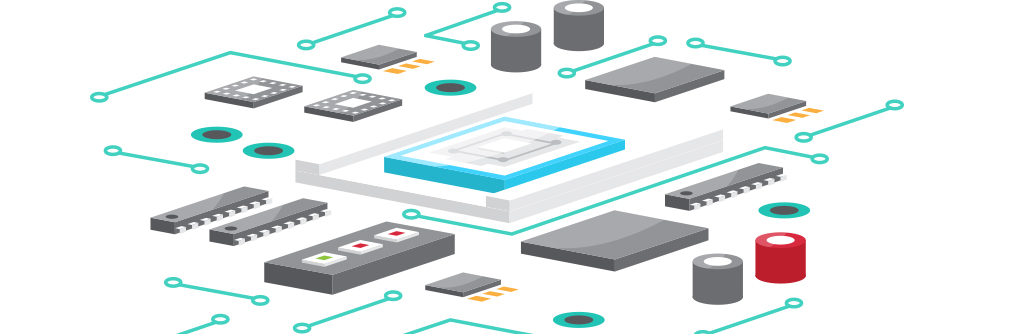
2. Semiconductor Design Engineer
A Semiconductor Design Engineer is responsible for designing and developing semiconductor components and systems such as microprocessors, memory chips, and integrated circuits. They work closely with other engineers, including process engineers, to ensure their designs can be manufactured using existing or new production processes.
The job role of a Semiconductor Design Engineer can vary depending on the specific industry and company they work for, but generally, their duties include:
- Developing and implementing semiconductor design methodologies, processes, and standards
- Designing and testing semiconductor components and systems using CAD tools and simulation software
- Collaborating with cross-functional teams, including process engineers, testing engineers, and project managers, to ensure successful design and product development
- Conducting feasibility studies and analysing technical requirements to guide design decisions
- Ensuring that designs meet performance, power, and cost targets while adhering to quality and safety standards
- Preparing and reviewing design documentation, including schematics, layouts, and test plans
- Troubleshooting and resolving design-related issues to ensure successful product development and release
Some of the skills required for a Semiconductor Design Engineer include:
- Strong understanding of semiconductor design methodologies, processes, and standards
- Proficiency in CAD tools and simulation software for designing semiconductor components and systems
- Familiarity with semiconductor manufacturing processes and their impact on design
- Experience in designing and testing complex semiconductor systems
Overall, a Semiconductor Design Engineer ensures that semiconductor components and systems are designed to meet performance, cost, and quality targets while adhering to safety and regulatory standards.